


Abstract
We present an open-source hardware and software ecosystem for optical atomic clocks. We provide PCB schematics and fabrication files for manufacturing the most important electronic systems together with the required software. The boards are designed for an active bad-cavity superradiant strontium clock and a passive optical lattice strontium clock, but they can be easily adapted to other atomic species' optical atomic clocks or ultra-cold atoms' systems like magneto-optical traps or Bose–Einstein condensate setups.
Export citation and abstract BibTeX RIS

Original content from this work may be used under the terms of the Creative Commons Attribution 4.0 license. Any further distribution of this work must maintain attribution to the author(s) and the title of the work, journal citation and DOI.
1. Introduction
Experimental systems in atomic, molecular and optical physics demand more and more complex and sophisticated requirements to see subtle effects like searching for dark matter [1, 2], Bose–Einstein condensates [3, 4], gravitational wave detection [5], spectroscopy of ultra-narrow transitions [6, 7] and other ultra-cold atom experiments [8, 9]. Among them, one of the most dominant examples is optical atomic clock experiments [6]. In realising such high-accuracy measurements, various non-standard solutions not available on the commercial market must be implemented. The most challenging is the design of electronic elements that can produce stable radio frequency or magnetic field pulses. Another common problem is adapting these devices to work with experiment control systems such as Sinara/ARTIQ [10]. Usually, a local electronic workshop is employed to prepare electronic devices and systems that are unique to only one particular experiment within a group. With their unprecedented precision, optical atomic clocks need many custom-made components to drive experiments correctly. While most existing laboratories have developed their own solutions for operating complex optical clocks, there are few papers that report their electronic circuits in detail [11–14]. At the same time, autonomously operated optical atomic clocks are becoming more common and in demand for new technology applications [15–17] and the new definition of the SI second [18, 19].
In this paper, we present an electronic system aimed at supporting the operation of optical clocks. While the electronic components presented here are designed for optical atomic clocks, they are also suitable for many other types of ultra-cold atom experiments, such as Feshbach resonance spectroscopy [20], optically pumped magnetometers [21], cold atom gravimetry [22] and quantum computing [23]. The presented electronic devices are suitable for both present-generation passive optical lattice atomic clocks and future-generation continuous active optical clocks based on superradiance [24–27]. They are composed of high-current drivers for controlling the magnetic field coils, a relocking system for the lasers' frequency stabilisation, direct digital synthesizer controllers, a phase and frequency comparator for laser–laser or laser–optical frequency comb (OFC) relative locks, and a cooling fluid flow-based interlock control circuit. Most of the presented devices can be configured using Ethernet and fast-switched using analog or transistor-transistor logic (TTL) signals. The designs are adapted to the electronic components currently available on the market.
All presented components are open-source hardware and software. In the open data repository we provide all PCB schematics and fabrication files required to manufacture the most important electronic systems together with the required software.
2. Components
2.1. Magneto-optical traps and offset field controller 15 A/100 A
Collecting atoms into optical lattices requires first laser cooling them down to several tens of µK temperatures. This is commonly performed in magneto-optical traps (MOTs) [28–30]. A quadrupole magnetic field, used in the MOT, is usually generated by a pair of anti-Helmholtz circular coils. Laser cooling and trapping of strontium are generally realised in two consecutive MOTs operating on two different atomic transitions [31, 32]. Therefore, two different values of current flowing through the coils need to be optimised in each of the MOTs, and ramping of the magnetic field gradients is required. This, together with fast turning on and off of the field, must be provided by the current controller.
Operating an optical lattice strontium clock after loading atoms into the lattice requires a static and homogeneous magnetic field either for defining a quantisation axis for the atoms and resolving clock transition hyperfine components needed for optical pumping and clock interrogation in fermionic  Sr isotope or for magnetic-induced spectroscopy [33] in the bosonic
  Sr isotope [6].
The aforementioned conditions require the capability to switch the direction of the current in one of the coils to move from an anti-Helmholtz configuration to a Helmholtz configuration.
In the case of a passive optical lattice strontium clock, the presence of the magnetic field induces systematic shifts to the atomic clock line, such as first- and second-order Zeeman shifts. The achievable stability of the magnetic field determines the uncertainty of these systematic shifts and, thus, the clock's accuracy. Moreover, the fluctuations of the magnetic field will directly deteriorate the clock's stability.
In a first-order Zeeman shift, a magnetic field, B, gives a linear shift of the sub-levels, which for π-transitions ( ) shifts the transition frequency, f, by
  , where µB
is the Bohr magneton and ge
and gg
are the g-factors of the excited and ground state, respectively. For
, where µB
is the Bohr magneton and ge
and gg
are the g-factors of the excited and ground state, respectively. For  Sr, a linear Zeeman shift has been determined experimentally to be
  Hz μT−1 [34].
A second-order Zeeman shift determination depends on the structure of the atomic levels, and in the case of strontium, the shift is dominated by the interaction of the excited triplet clock state with the other nearest triplet state,  , where
  is the energy separation between the two triplet states.
For strontium, the quadratic Zeeman shift is  Hz μT−2 [35].
Assuming  60 μT in state-of-the-art
  Sr clocks [35, 36] a fractional accuracy of 10−18 requires a stability of the B field better than
  0.000 087 μT, i.e.
  . For a bosonic
  Sr clock, the bias field is usually higher, for instance
  210 μT in one of the best transportable clocks [37]. There is, however, no linear Zeeman shift. The quadratic Zeeman shift sets the requirements
  0.04 μT, i.e.
  .
.
In contrast to passive clocks, an active superradiant clock uses the radiation collected directly from the clock transition as a reference. The atoms are correlated in the superradiant emission, creating a collective atomic dipole. To a first approximation, superradiance may occur if the relative frequency shifts,  , between atoms are below the atomic line width. The space and time inhomogeneity,
  , of the magnetic field applied to the ensemble of superradiating atoms leads to different frequency shifts of the upper lasing state. For the 1 mHz line of fermionic
  Sr and a field of 60 μT the field's required space and time homogeneity due to the linear Zeeman shift is on the order of
  . In the bosonic isotope
  Sr the induced line width is extremely small and depends quadratically on the value of the offset field B [38]. For instance,
  T induces a line width of
  nHz. Therefore, the quadratic Zeeman shift imposes extremely high space and time homogeneity requirements at the level of
  .
.
However, as was shown in [39], the superradiance of an atomic ensemble in a bad-cavity regime is allowed for less restrictive conditions, i.e.  , where N is the number of atoms, g is the coupling strength of the lasing transition with the cavity mode and κ is the decay rate of the cavity field. Based on this, one can estimate the required homogeneity of the magnetic field over the atomic ensemble. For instance, for 10
 Sr atoms collected in a cavity with a finesse of 105, the estimation yields
  .
.
A finite-element method simulation of the magnetic field homogeneity for a magnetic field generated from in-vacuum coils surrounded by Mu-metal shields is presented in figure 1. It shows that such homogeneity is possible even with the highly inhomogeneous field from MOT coils present just outside the shields. This particular setup is designed for an active continuous optical clock based on the idea of a moving magic-wavelength lattice scheme, as proposed in [26, 40].
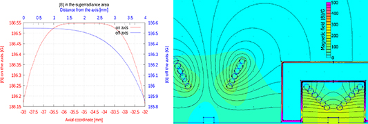
Figure 1. Magnetic field distribution simulations for the set of MOT field coils and bias field coils for the superradiance experiment. The superradiant area is surrounded by a magnetic shield. Left: Numerical simulations of the magnetic field in the area of superradiance performed for the following parameters: I = 40 A, six windings per coil, internal radius 8 mm, distance between coils 4 mm, copper wire thickness 3.175 mm, permeability of the shields 87 000, thickness of the shields 1 mm. The external magnetic field generated by the MOT coils has been taken into account. Right: Distribution of the magnetic field in the MOT and superradiance area (inside of a two-layer magnetic shield, shown in the bottom-right). Cross-sections of the Mu-metal shields and copper windings are visible.
Download figure:
Standard image High-resolution imageThe device presented schematically in figure 2 has two separate controllers, for currents up to 15 A and 100 A, respectively, to increase resolution in the low-current regime. The active controller is selected by a TTL signal. A block diagram of a controller is presented in figure 3 on the basis of the 100 A controller. An output current is set by analogue input. The analogue signal is converted to digital and digitally filtered to remove any input noise. A digital proportional-integral-derivative (PID) controller and a digital–analogue converter (DAC) stabilise the current output sensed by a LEM IT 200S Ultrastab current sensor. The digital–analogue converter is referenced to an external ultra-stable ADR4540BRZ voltage reference with the relative noise below  and relative temperature drift coefficient below
  C−1. Both or only one of the coils can be connected by an H-bridge to allow changing of the current direction in both coils, or only in one of them, enabling switching between Helmholtz and anti-Helmhotz configurations. The full PCB schematics together with fabrication files for the PCB design and manufacturing are available at [41, 42].

Figure 2. Concept of 15 A/100 A current controller.
Download figure:
Standard image High-resolution image
Figure 3. 100 A part of the current controller.
Download figure:
Standard image High-resolution image2.2. Compensation coils controller ( A)
A)

In any cold atom experiment, precise control over the magnetic field is necessary. It is especially important to have a 3D control to compensate for the Earth's magnetic field and any stray magnetic fields in the laboratory. On the other hand, transferring atoms between different traps, such as between a MOT and an optical lattice, is usually enhanced by adding static offset fields, for instance to compensate imbalances of laser light intensity in retro-reflected beams. Three pairs of different Helmholtz coils usually ensure all these conditions. Due to experimental space constraints, usually the pairs are not identical and require different currents.
The current controller for the compensation coils should be able to tune the currents' values and change their directions independently for each pair. Assuming that the Earth's and stray magnetic fields are below 100 μT in each direction, a fractional clock accuracy of 10−18 requires the same level of stability of the magnetic field as described in the previous section.
The presented device can be programmed by Ethernet connection over Telnet protocol. Programming allows presetting in memory 32 values of the current on each of the compensation coils. Fast addressing and setting the output values is performed by TTL signals (five addressing bits and one clock/set bit). An output in the range of −3 A to 3 A is provided by a 16-bit digital–analogue converter stabilised to the ultra-stable ADR443BRZ voltage reference. Additionally, an arbitrary-length linear ramp can be programmed, triggered by a clock/set TTL.
A conceptual diagram is presented in figure 4. The full PCB schematics and fabrication files for the PCB design and manufacturing are available at [43]. For each channel, the current is stabilised to the digital–analogue converter output by sensing the current using high-quality shunt resistors. The coils are connected through a TTL-controlled H-bridge.
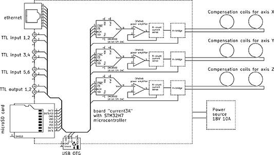
Figure 4. Compensation coils controller. © 2022 IEEE. Reprinted, with permission, from [44].
Download figure:
Standard image High-resolution imageWe also provide open-source software (see appendix
2.3. Autonomous relocking system
The operation of an optical clock depends on the simultaneous correct operation of many subsystems, including dozens of systems for precise stabilisation of the lasers' frequencies to external references such as spectrometers, optical cavities, OFCs and atomic lines. As a result of mechanical, thermal and electrical disturbances, laser controllers may lose their optimal working conditions and remain in a state that makes it impossible to maintain the lock, thus interrupting the clock's operation. The remedy for this type of issue is an electronic autonomous relocking system. Most of the time, their operation is based on continuous observation of selected signals, detecting an approaching unstable working condition and correcting the settings of the appropriate device, as necessary. However, if a loss of lock is detected, an attempt is made to restore the lock, and the event is added to a log.
In a real system, each laser has individual operating parameters, behaviours and relocking algorithms. Therefore, the relocking device should be based on a programmable setup. Both the output and input signals could be analogue or digital (an example of digital input signals may be data from a wavelength meter or an OFC); therefore, analog to digital converters (ADC) and digital to analog converters (DAC) are required as well as digital communication ports.
We have developed a compact ADC/DAC card compatible with a Nucleo-H743ZI2 board (figure 5). By default the card is adapted to work with Toptica external cavity diode laser (ECDL) drivers, but it may also be used with other devices. The card requires a +/−15 V power supply delivered from the controlled device to avoid electrical disturbances. The signal from the analogue input port is amplified and directly connected to the built-in microcontroller 16-bit ADC converter. The input signal is used to observe transmission through the optical cavity and detect the loss of a lock by the signal falling to zero. When used with an injection-locking system [45], the transmission signal can be observed through an optical filter. It can also be used to monitor for single/multi-mode laser operation when used with a Fabry–Pérot interferometer. The analogue output signal is generated by the built-in microcontroller DAC converter, and then, with the use of operation amplifiers, the range of generated voltages is extended to −3 V to 3 V instead of the 0 V to 3 V range produced by the microcontroller. Operating around zero voltage is of great practical importance and allows the device to be easily switched from automatic to manual operation. The board is equipped with manual switches allowing for smooth connection and disconnection to an already working laser driver. Output analogue signals are usually used for slow compensation of laser diode current or external cavity piezo voltages with modulation ports on the laser drivers, which are very sensitive to any electrical noise. For this reason, a low-pass filter is used to cut potential high-frequency noise derived from the DAC.
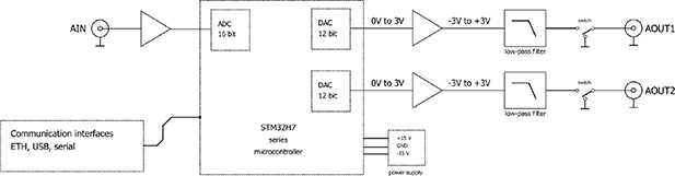
Figure 5. Relock board.
Download figure:
Standard image High-resolution imageThe Nucleo-H743ZI2 board is equipped with an Ethernet communication port, which extends the functionality of the relock board. The board can act as a remote DAC and ADC controlled via a local network if the relocking algorithm is run on a computer in the lab. On the other hand, the relocking program (written in the C language) can be run on the microcontroller, making the system autonomous. In this case, Ethernet connectivity is very useful, for example if data from a wavelength meter is required.
The complete PCB schematics and fabrication files for the PCB design and manufacturing are available at [46].
2.4. Direct digital synthesizer controller
Many parts of optical clocks require precise control of the laser frequency. This is especially important in clock transition spectroscopy, for capturing cold atoms in optical traps, when operating on the magic wavelength, for frequency transfer and for conversion from the optical to the RF domain. For all of these tasks, acousto-optical modulators or electro-optical modulators driven by RF generators are used. Therefore, precise frequency generators are essential. For the best performance, the resolution of the frequency control should be on the order of the μHz level, with the possibility to use an external precise clock, such as a H-maser, as a reference. It is often required to switch between different frequencies in a short time (i.e. less than 1 μs) and to have the ability to change parameters by other programs via a LAN network. Most of the frequency generators available on the market do not meet all these requirements, and custom solutions are needed. Commercial direct digital synthesizer evaluation boards from Analog Devices (such as the AD9912 or AD9959) have proven to be a good choice. However, they need to be controlled via fast serial peripheral interface (SPI) interfaces.
We have developed a compact module compatible with the AD9959 and AD9912 evaluation boards based on a microcontroller, which significantly extends the capabilities of these boards, makes them easier to use and has the vast majority of the functionality needed in an optical atomic clock laboratory. A schematic of the device is presented in figure 6. The module communicates with the direct digital synthesizer (DDS) board via the fast SPI. It is equipped with an Ethernet port, allowing easy control of the device from anywhere in the laboratory (see appendix

Figure 6. Block diagram of the direct digital synthesizer controller.
Download figure:
Standard image High-resolution imageThe full PCB schematic of the comparator, together with the required fabrication files for manufacturing and software for the microcontroller, are available at [49, 50].
2.5. Phase and frequency comparator with frequency divider
A phase and frequency comparator is an indispensable component whenever the laser beam frequency stabilisation step employs beat-note detection and a phase-locking setup. In passive optical atomic clocks this includes stabilisation of lasers to an OFC [51, 52], phase stabilisation between two lasers by optical offset phase locking [53, 54] and active Doppler shift cancellation in optical fibres [47, 48].
In an active optical clock based on superradiance, a phase and frequency comparator is necessary to provide the length stabilisation of the superradiant cavity. To achieve superradiance conditions in a bad-cavity regime, one of the optical cavity modes has to be tuned to the atomic transition frequency. A superradiant cavity that can sustain superradiance in both fermionic  Sr and bosonic
  Sr isotopes of strontium requires a finesse on the order of 100 000. Assuming a length of 15 cm, the full width at half maximum of the cavity mode is 5 kHz. This implies that the frequency of the chosen mode of the cavity has to be tuned and stabilised with a precision of 1 kHz or better. The cavity mode frequency is determined by the cavity length, and the length, in turn, can be locked to some external laser [55] with absolute frequency stability. Tuning can then be achieved with an acousto-optic modulator (AOM) and stabilisation to an external reference, such as the OFC.
A simple offset lock for the laser frequency to an OFC is depicted in figure 7. An error signal for laser stabilisation is generated by comparing the phase difference between a stable RF generator and an optical beat note between the OFC tooth and the laser. A phase difference detection is made by a phase and frequency comparator with a variable dividing the ratio of the input frequency signal. This frequency divider allows adjustment of the sensitivity of the system. The generated error signal is applied through a PID controller to the laser.
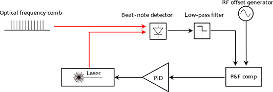
Figure 7. A simple offset lock to an optical frequency comb with a phase and frequency comparator.
Download figure:
Standard image High-resolution imageA schematic diagram of a comparator is presented in figure 8. A digital phase frequency detector (HMC439QS16G), used in our comparator, provides an output voltage proportional to the phase difference between the inputs when this difference is smaller than  . For higher phase differences, the output voltage saturates at the positive or negative value, depending on which input frequency is higher. This particular property provides a high capture range for the lock system. The values of the frequency dividers are set over a SPI from a simple microcontroller. The microcontroller itself is programmed manually by two arrays of jumpers. The full PCB schematic of the comparator together with the required fabrication files for manufacturing and software for the microcontroller are available at [56].

Figure 8. Phase and frequency comparator.
Download figure:
Standard image High-resolution image2.6. Water flow sensor interlock
In both active and passive optical atomic clocks, the high-current coils require water cooling. This includes MOTs and offset coils, and the Zeeman slower coils if not based on permanent magnets. Overheating of these coils can be catastrophic to the experiment. An interlock control circuit verifying the returning water flow provides an instantaneous fail-safe protection by turning off the power supply.
Figure 9 presents a diagram of the device. The interlock control's design is kept simple on purpose, and any faults in its operation should switch off the power supply to prevent overheating of the coils. Flow sensor impulses are converted to voltage, and this voltage is compared by a differential amplifier with a pre-adjusted discriminating level. The output of the differential amplifier is sent through a flip-flop latch to a relay that changes the interlock state in a power supply. If the flow drops below the discriminated level, the latch will cut the power to the relay, and will not bring it back online before a human operator checks the system and resets the flip-flop latch. The complete PCB schematic of the interlock sensor together with the required fabrication files for manufacturing are available at [57].

Figure 9. Diagram of a flow sensor interlock.
Download figure:
Standard image High-resolution image3. Conclusions
In this paper, we detail an open-source hardware and software ecosystem designed for optical atomic clocks. These designs include a wide range of electronic circuits optimised for precision control of magnetic fields (controllers up to 100 A and compensation coils), maintaining and distribution of frequencies (relocking system for lasers, DDS controller, phase and frequency comparator), and for water cooling (water flow sensor interlock). The presented systems allow us to meet the challenging conditions required in passive and superradiant active optical atomic clocks. They are also suitable for many other ultra-cold atom experiments.
Acknowledgment
This work was supported by the European Union Horizon 2020 research and innovation programme, Quantum Flagship Project No. 820404 'iqClock' and No. 860579 'MoSaiQC'. This project has received funding from the EMPIR programme co-financed by the Participating States and from the European Unions Horizon 2020 research and innovation programme. It has been supported by the EMPIR project 18SIB05 'Robust Optical Clocks for International Timescales.' The presented work was performed at the National Laboratory FAMO (KL FAMO) in Toruń, Poland, and was supported by a subsidy from the Polish Ministry of Science and Higher Education.
Data availability statement
The data that support the findings of this study are openly available from the following sources: [41–43, 46, 49, 50, 56, 57].
Appendix A: Software for the compensation coils driver
The compensation coils driver is programmed by presetting into its memory the values of the output currents over the Telnet protocol. During operation, the output currents can be changed between preset values by input TTL signals. This method is compatible with DIO cards and RT computers used in the laboratory environment to control experiments. Additional parameters stored in the memory together with current values allow either fast switching between desired levels or a linear ramp of arbitrary time.
A.1. Pre-programming memory
The format of commands used in Telnet programming is

 where 'parameter address' sets the logical address in the memory , 'valueX' are the preset current values for the respective coils, and 'time' is the length of a linear ramp in milliseconds; a value of 1 means the fastest possible switching.
Multiple parameters may be set with a single command by separating them with an '&' sign:


Two additional commands may used to get help and to close the connection:
help
exit
The most common parameters and addresses are presented below:
.
| DAC: 000 | set values for memory 1 |
|---|---|
| DAC: 001 | set values for memory 2 |
| DAC: 010 | set values for memory 3 |
| 000 | address of memory 1 |
| 001 | address of memory 2 |
| 010 | address of memory 3 |
© 2022 IEEE. Reprinted, with permission, from [44].
After making a connection, if the connection is successful a help message will be sent by the driver. This message guides the operator how to communicate with the driver. For example, the command to pre-program the first two memory values is
DAC: 000: −1.25 684; 0.5; 0.0; 1; & 001: 0.52; −2.1; −1.0; 50;
Switching to the first memory (000) levels takes 1 ms, while switching to the second memory levels (001) is made using a 50 ms long linear ramp.
A.2. Switching between pre-programmed levels
In the current version of the software, switching between pre-programmed values is made by four TTL signals, but it can be easily expanded to use all six available TTL inputs. Three TTL signals address the required memory, and one TTL is a set/clock signal that triggers switching outputs to the new memory levels. TTL 1 is the least significant bit, and TTL 3 is the most significant bit [44].
For instance, the following pattern switches the controller output to the pre-programmed value stored in memory location 2 (001).

Appendix B: Software for dds
The device is controlled by setting the appropriate parameters using the Telnet protocol. The format for writing the parameters is
 .
.
Multiple parameters may be set in one command by separating them with a ';' sign:
 .
.
The command bellow is used to read the value of a parameter:

The most common commands are presented below:
| DDS:CH0:FREQ | set frequency of the ch0 dds output (value in MHz) |
|---|---|
| DDS:CH0:AMP | set amplitude of the ch0 dds output (value from 0 to 1) |
| DDS:CH0:PH | set phase of the ch0 dds output (value in deg) |
| SCAN:ON | turn on/off (value 1/0) the frequency scan |
| SCAN:RANGE | scan range in MHz |
| SCAN:STEP | scan step in MHz |
| SCAN:CH | the number of the dds output channel on which the scan is performed |
| SCAN:GNDCMP | turn on/off (value 1/0) removing background form spectroscopy (additional setup driven by TTL for turnning on and off the signal required) |
| SCAN:VOLT | the value of the measured signal (value in bits of ADC) |
| SCAN:DT | dead time between setting the frequency and measurement |
| DLOCK:ON | turn on/off (value 1/0) digital lock |
| DLOCK:JUMP | amplitude of frequency detuning for digital lock |
| ADC:CH0:AVR | number of ADC measurements executed for voltage measurement (the value is an average of ADC measurements) |
For each of the parameters, apart from the value, one can set the maximum and minimum value and enable saving of the parameter values to the microcontroller memory with the following commands:
 : maximum allowable value of the parameter.
 : minimum allowable value of the parameter.
 : turn on/off (value 1/0) saving data to memory.
 : size of the table in memory.