

Abstract
Two-dimensional (2D) transition metal borides, have recently attracted tremendous interest and become an emerging class of 2D materials due to their intriguing properties. We report systematic investigation of stability, electronic properties and optical activity of 2D-TiB2 nanosheets using first-principles calculations. By combining elastic and phonon-dispersion calculations, we substantiated the mechanical and dynamic stability of 2D-TiB2 nanosheets. Our results of elastic calculations reveal that addition of an extra layer destroys the auxetic behaviour of monolayer (ML) 2D-TiB2 with significant reduction in the brittleness. Further, based on the spin-polarised electronic structure calculations, we find that a low-dimensional metallic state of ML can be achieved by tuning the distance between the titanium and boron layers. The calculations clearly reveal that metallic nature does not destroys the auxetic behaviour of ML. Subsequently, we investigated the optical response of 2D-TiB2 nanosheets (ML and bilayer (BL)) at the level of density functional theory and many-body perturbation theory. The results obtained by solving Bethe–Salpeter equation (GW+BSE formalism) shows that excitonic effects causes a slight blue-shift in the absorption spectra of the nanosheets with ML being optically active with sharp peaks in infrared (IR) and ultraviolet (UV) regions while BL shows the reduced optical activity across wide range of photon energies spanning the near-IR to UV region. In addition, electronic polarisability of the nanosheet decreases with addition of another layer in ML 2D-TiB2. Further investigation of transition probabilities clearly indicates that the response of ML at Dirac point is tunable by spin–orbital coupling effects which makes these nanosheets promising for spintronic applications. The BL exhibits distinct electronic, and optical properties compared to ML. Our study unravels the structural, elastic, electronic, and optical properties of 2D-TiB2 nanosheets and suggests them as promising candidate for variety of optoelectronic and spintronic applications.
Export citation and abstract BibTeX RIS
1. Introduction
Nanoscience is the emerging field and has been providing solutions to bottlenecks for a decade. The two-dimensional (2D) materials have gathered a large interest mainly due to the novel behaviour of electronic systems and unusual physical phenomena that occur when charge and heat transport is confined to a plane [1]. Novoselov et al [2] reported single-layer graphene and exfoliated 2D materials from van der Waals (vdW) solids exhibiting unique and intriguing physical properties, while the discovery of graphene (2D monolayer (ML) of carbon atoms), has brought up a famous category of 'Dirac Materials', referring to the lattice systems where excitations are described by relativistic Dirac equations [3]. These are generally semiconductors where two (or more) bands get strongly coupled near a level-crossing [3]. Long ago Frindt et al has shown that layered structures can be exfoliated (mechanically and chemically) into few and single layers [4–8]. Shortly after graphene, 2D hexagonal boron nitride (h-BN) realised as an ideal substrate for graphene electronics [9, 10] as it induces a bandgap in graphene when graphene was deposited onto it [11]. Reducing the carbon footprint, focus drifts towards 2D materials beyond graphene ranging from semiconductors to insulators to metals and even to superconductors [9], such as h-BN [12], semiconductor monoelemental analogues of graphene, graphane (the sp2, H-terminated sp3 derivatives) like silicene [13–15], germanane [16], phosphorene [17] and semiconducting transition metal di-chalcogenides (TMDs) [18]. Distinguished from vdW materials, MAX phase (layered transition metal carbides/nitrides) derived 2D transition metal carbides/nitrides labeled as MXenes [19, 20], have gained much interest for promising applications in batteries, hybrid electro-chemical capacitors, catalysis, spintronics and flexible devices [20]. Boron, being the nearest neighbour resembles carbon in its capability to form molecular networks [21]. Guo et al [22] first reported 2D transition metal boride (referred to as MBenes based on 2D morphologies) derived from layered MAB phases with the formula of  (M can be Cr, Mo, W, Fe, Mn or their solid solutions and B is boron). Transition metal borides are extensively studied in their bulk form, however the studies of their low-dimensional analogues in the form of nanoflakes, nanosheets, and nanotubes are still in the nascent form. 2D family of materials have seen rise with the advent of graphene [2], followed by TMDs [18], h-BN [9, 10], Xenes (borophene, aluminene, gallene, indiene, etc) [13–15], MXenes (transition metal carbides, nitrides or carbonitrides) [19, 20], and youngest member of 2D family MBenes (2D transition metal borides) [23]. Extensive reviews on MBenes [23–27] unravels that these novel 2D materials are sparking interest in material science and condensed matter community. Titanium diboride (TiB2) is a hard ceramic that shows excellent heat conductivity and wear resistance in its bulk form [28]. It possesses high elastic modulus (about 565 GPa) [29], high hardness (about 25 GPa [29], Vicker's), and high flexural strength (about 400 MPa [29]) in its bulk form that are indispensable in specialised applications [30]. In the search for Dirac materials beyond carbonic and topological members, TiB2 has been an excellent candidate, wherein the ML TiB2 is shown to host Dirac states, exhibiting Dirac cones near to the fermi level (
 ) at an off symmetry point [31]. Under the umbrella of MBenes family, 2D TiB2 finds its immediate applications in energy storage and electrocatalytic reactions. Presence of dirac states near fermi level and graphenelike band structure further opens up the avenue for the topological studies of TiB2, which is limited in other 2D materials. Further Yi et al [32] have observed nodal rings on the orthogonal
  and
and  planes of the Brillouin zone (BZ) in TiB2, based on angle-resolved photoemission spectroscopic studies. They also observed surface states on the (001) cleaved surface of TiB2 which motivates further studies about its topological signatures contrasting from other 2D materials. Further Feng et al [33] have shown in their recent work that TiB2 and ZrB2 are tunable by spintronic effects, where dirac nodal-net semimetallic state can be realised in absence of spin–orbital couplings (SOCs). Specifically in TiB2 several topological novel states (such as triple point, nexus, and nodal link) can be realised which are co-protected by spatial-inversion and time-reversal symmetry. Also analogous to ML and bilayer (BL) graphene, 2D surface dirac points are realised on (001) surface. In their recent work Sevik et al [34] have shown that in similar class of materials (Ca, V, Nb, Ta, Sc) B2, high temperature superconductivity can also be harnessed by means of metal doping in boron honeycombed network which is clearly distinct from all other exisiting 2D materials providing such materials an edge to compete with other 2D materials for their experimental manifestations. The dimension reduction in TiB2 (from bulk to 2D) is accompanied by reduction in in-plane lattice thermal conductivity at room temperature, which is completely opposite of the expected trend for MoS2, MoSe2, WSe2 and SnSe [35]. Recent work reveals that TiB2 derived nanosheets can act as additive to enhance CO2 capture of calcium oxide (CaO)-based materials, where addition of 1% of TiB2 nanosheets can lead to enhancement of CaO capturing capacity up to 25% [36]. Further, it is also reported that the vacant sites in delaminated TiB2 nanosheets can be utilised for nitrogen adsorption without any energy expense [37], which can lead to the use of TiB2 nanosheets for nitrogen fixation. Such works arouse the interest in 2D titanium borides for their fundamental understandings. Such intriguing properties of 2D TiB2 motivates for its experimental synthesis, where several research groups have tried to synthesise 2D nanosheets of metal diborides [38]. Yousaf et al reports the synthesis of flat, planar sheet of quasi-2D TiB2 (and other metal diborides) using ultrasonication-assisted direct liquid-phase exfoliation [38]. Other fabrication methods involves mechanical exfoliation and chemically induced selective extraction [39]. Further experimental synthesis efforts for 2D metal borides are included in detail in our recent review article [23].
In this paper, using density functional theory, we investigate the 2D TiB2 ML (single layer) and BL (two layers stacked in z direction) for their structural and dynamical stability, mechanical robustness and elastic properties, electronic structures, and the opto-electronic properties. The present article aims to unravel the new science and novel properties of 2D materials beyond graphene where novelty lies in the findings about ML and BL TiB2. Theoretical studies reveal the stability of the nanosheets by means of phonon-dispersion and mechano-elastic calculations. Our findings indicate the disappearance of auxetic behaviour in BL mainly accounted to the enhanced in-plane stiffness. Further, we find that both ML and BL are of brittle nature, while with the addition of a single layer (as in BL) the brittleness has been drastically reduced. Furthermore, we show that with the increase in distance between titanium and boron layers, linear valence band crosses the fermi level, forming a low-dimensional metallic state of ML. Then, we solve Bethe–Salpeter equation (BSE) on top of GW (where single particle Green's function G and the screened coulomb interaction W is treated at the level of GW0+BSE) to obtain the optical spectrum of ML and BL including many-body effects. We find that excitonic effects cause a slight blue-shift of the density functional theory (DFT) calculated optical spectra (without electron–hole interactions) for both ML and BL. Further, ML is optically active with sharp peaks in infrared (IR) and ultraviolet (UV) regions, with BL showing reduced optical activity across wide range of energies spanning the near-IR (NIR) to UV region. Also, the electronic polarisability of the nanosheet decreases with additional layer (as in BL). Finally, the calculations show high transition probabilities of ML at Dirac point which are tunable by spintronic effects (SOC) which makes these nanosheets suitable for optoelectronic and spintronic device applications. As this emergent 2D transition metal diborides family stems from diverse family of non-vdW materials, it is manifested to advance the field many-fold for application based needs.
2. Theoretical methods
2.1. Mechanical and elastic framework
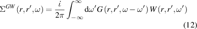
In this section, we have explained the theoretical model utilised to calculate the mechanical and elastic parameters. Generally stress–strain method is used to obtain elastic constants, where the stress response (σ) corresponding to strain (ε) can be modelled as
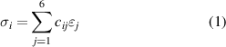
The stress (σ) and strain (ε) are vectors having 6 independent components ( ). C
). C is second order elastic stiffness tensor expressed by a 6 × 6 symmetric matrix in units of GPa. The elastic stiffness tensor C
 can be determined based on the first-order derivative of the stress–strain curves. This method is, however quite computationally expensive, hence in the present study, elastic constants have been determined based on the energy–strain method, where energy variation corresponding to small applied strains to the equilibrium lattice configuration are recorded [40]. Under harmonic approximation, the elastic energy (
 )of a solid is given by
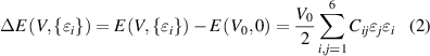
where  and
and  represents the total energies of distorted and equilibrium lattice cells, with volume V and V0, respectively. In this method the elastic stiffness tensor (Cij
) is obtained from second-order derivative of total energy versus strain curves [40]. Polynomial fitting procedure for calculating the second derivative at the equilibrium of the energy with respect to the strain is applied [41].
represents the total energies of distorted and equilibrium lattice cells, with volume V and V0, respectively. In this method the elastic stiffness tensor (Cij
) is obtained from second-order derivative of total energy versus strain curves [40]. Polynomial fitting procedure for calculating the second derivative at the equilibrium of the energy with respect to the strain is applied [41].
Laue classes of the hexagonal crystal system has the following form of the elastic matrix (Cij
) with five independent elastic constants in its bulk form (space group 191, P6/mmm, hP1), where one of the element (C66) can be expressed as combination of other independent elements ( ) [42]
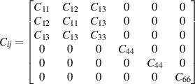
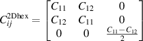
In 2D realm, only two independent elastic constants (C11 and C12) have been realised for hexagonal system, as the elastic matrix reduces to 3 × 3 form as follows [41]
Born stability conditions [42] for hexagonal crystal system (bulk) have quadratic stability criteria as follows:
Criteria I: 
Criteria II: 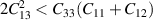
Criteria III: 
Criteria IV: 
However the criteria of mechanical stability in 2D realm [42–44] requires  and
and  .
.
Further, the linearly varying elastic properties of 2D materials are mainly characterised by in-plane stiffness (C) and Poisson's ratio (ν), where C is determined by linear elastic constants and ν is the ratio between transverse contraction strain and longitudinal extension. For 2D hexagonal system, there are two different strain modes for which the strain vector (ε) is (δ, 0, 0) and (δ, δ, 0), respectively and the corresponding elastic energy ( ) is
) is  and
and  , respectively. C11, C22, and C12 represents the elastic stiffness along xx, yy, and xy directions, respectively. In 2D hexagonal nanosheets elastic stiffness along xx and yy directions is similar (
 ). So for 2D hexagonal nanosheets, in-plane stiffness C and Poisson's ratio ν can be expressed in terms of elastic strain tensor elements, Cij
as
). So for 2D hexagonal nanosheets, in-plane stiffness C and Poisson's ratio ν can be expressed in terms of elastic strain tensor elements, Cij
as
2.2. Optical framework for 2D materials: DFT and GW-BSE formalisms
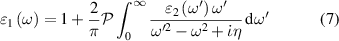
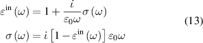
In this section we have detailed underlying theoretical methods to understand light–matter interaction and calculate optical properties of the 2D nanosheets. The linear optical properties can be obtained from frequency dependent complex dielectric function  calculated in the framework of the independent-quasiparticle approximation [45], defined as:

where  and
and  are the real and imaginary parts of the dielectric function, and ω is the photon frequency. Frequency dependent imaginary part
  can be calculated from dielectric matrix which is calculated from the electronic ground states by a summation over empty states [46] as
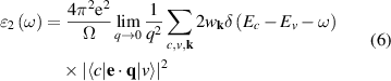
where indices c and v corresponds to conduction and valence states and  corresponds to the integrated optical transitions from valence to conduction states, while e and q are photon's polarisation direction and electron momentum operator, respectively. The integration is carried out on k by summation over k-points with a carried weight factor wk
. Also, frequency dependent real part
corresponds to the integrated optical transitions from valence to conduction states, while e and q are photon's polarisation direction and electron momentum operator, respectively. The integration is carried out on k by summation over k-points with a carried weight factor wk
. Also, frequency dependent real part  can be calculated from the imaginary part
  by the Kramers–Kronig transformation [46] as
where  denotes the principal value and η is the complex shift parameter in Kramers–Kronig transformation which causes a slight smoothening of the real part of the dielectric function. Local field effects are however neglected in this approximation. Further from the real
  and imaginary
  parts of dielectric function, frequency dependent linear optical spectra of extinction coefficient
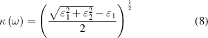
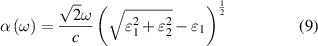
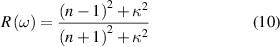
  , absorption coefficient
  , and reflectivity
  can be obtained [47] as follows, where n is the refractive index
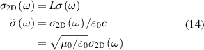
To take excitonic effects into account, we have employed the GW techniques to calculate the excited state properties. Based on GW-approximation, energies are calculated as

where  and
and  are GW quasiparticle energy and Kohn–Sham energy of the ith state, respectively, while
  is the self-energy of the ith state. Starting from standard DFT calculations for ground-state energy and electronic density, we calculated the linear optical spectra by solving BSE on the top of GW excited-state calculation (GW0 approximation). The self-energy (equation (12)) in GW approximation [48, 49] is product of Green's function and dynamically screened interaction
  , (
, ( ), which is the bare Coulomb interaction ν screened by dynamical dielectric function
Based on many-body quasiparticle framework [50, 51], GW formalism corrects the DFT based single electron eigenvalues by including exchange and correlation effects in self-energy term. The errors in determination of dynamically screened interaction  can be covered by including the solution of BSE performed on the top of GW calculations [52]. We have further utilised single-shot G0W0 approximation, where the screened Coulomb interaction W remains constant at its starting value while the one-electron Green's function G is self-consistently updated over the course of a single iteration. One could anticipate that the estimated optical characteristics via GW-BSE formalism will provide greater agreement with experiment.
The optical properties of 2D hexagonal layers are not properly treated using the macroscopic treatment as it incorporates the finite layer thickness (d = 0.3–0.7 nm for graphene [53]) in the limit of  . For low-dimensional 2D systems, the dielectric function depends on the considered thickness of the vacuum region (L). In periodic stack of layers (multilayered system), sufficiently large interlayer distance has to be kept to avoid interactions between the periodic images of the 2D nanosheet [54, 55]. In order to circumvent such thickness problem, the L-independent optical conductivity of 2D layer
  can be used to characterise optical activity of any layered 2D system [56, 57]. For the optical activity of 2D layers, we are interested in the in-plane component
  of the dielectric tensor, corresponding to light polarisation in a direction perpendicular to layer normal. For a freestanding 2D nanosheet (ML and BL) under the assumption of normal incidence, optical properties are mainly influenced by in-plane optical conductivity
  . Further the in-plane component of macroscopic dielectric tensor can be related to optical conductivity
  [58] as,
where ε0 is the vacuum permittivity and ω is incident wave frequency. In such formalism if we change our artifical three-dimensional model (containing vacuum layer) to 2D nanosheet, the in-plane 2D optical conductivity  [56, 59] relates as,
where L is the slab thickness in the simulation cell and  is normalised conductivity. Within independent-quasiparticle formalism, the dielectric function can be related to eigen states
  and eigen values
  by Ehrenreich–Cohen formula [60], to describe real part of 2D optical conductivity as,
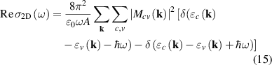
where A is the area of nanosheet and  is electric-dipole matrix element for interband transition [46], defined as,
where  is in-plane wave vector perpendicular to hexagonal axis, accounting for transitions between filled valence v and empty conduction c bands, and
  is Bloch matrix element of in-plane component of momentum operator. In 2D nanosheets, reflectance generally has a small value and in the limit of vanishing reflectivity [60], the absorbance of the nanosheet can be related to 2D optical conductivity as,
where µ0 is permeability of free space and c ( ) is speed of light. Similar to the real part of the dielectric function, Kramers–Kronig relations can be utilised to derive imaginary part of 2D optical conductivity from real part in equation (15), as
where  is cauchy principal value. For normal incidence, the optical properties of freestanding 2D layers in air, the reflectance R, transmittance T, and absorbance A independent of the light polarisation [56, 59] can be written as follows,
As the reflectance for 2D layers is extremely small, the absorbance (equation (21)) and the real part of the normalised conductivity (equation (17)) agree well and obtain similar values. Influence of frequency-dependent conductivity on optical properties of 2D layers is studied using above formalism. The dependency of the optical properties of 2D nanosheets on the band structure and electrical properties can be studied by calculating transition dipole moment (TDM), where the probability of an electronic transition is proportional to the square of the electronic TDM. For the transition between the initial a (valence) and final b (conduction) states in 2D nanosheets, the dipole transition matrix element which is the associated electric dipole moment, can be modelled as
where ψa and ψb are eigen states with Ea and Eb as their eigen energies andm is the electronic mass. The transition probabilities are calculated as the sum of the squares of TDM, P2, in widely accepted units of Debye2.
3. Computational methods
The calculations in this paper were carried out within the framework of DFT using the generalised gradient approximation with Perdew–Burke–Ernzerhof (PBE) exchange-correlation functional [61] and hybrid functional Heyd-Scuseria-Ernzerhof (HSE06) [62], as implemented in the Vienna ab initio simulation package [63, 64]. The structural models have been relaxed and optimised until the forces acting on the atoms are smaller than 0.01 eV Å−1. The Kohn–Sham orbitals are expanded on a plane-wave basis with an energy cutoff of 420 eV and the BZ has been sampled using the Monkhorst-Pack k-point mesh of  . In all the calculations, a 15 Å vacuum region is used perpendicular to the nanosheet (z-direction) to avoid any interaction between the nanosheet and its periodically repeated images of the unit cell. The elastic, mechanical, and electronic calculations have been carried out with the projector-augmented-wave method [65]. The phonon dispersion calculations are based on the PHONOPY code [66]. Second-order harmonic force constants have been calculated by the finite difference method, as implemented in the PHONOPY package [66]. The ab-initio molecular dynamics (AIMD) simulations utilise a canonical ensemble and a Nosé–Hoover temperature control at room temperature (300 K) for 3 ps [67]. To ensure convergence criteria, we have used the
  q-mesh to obtain the phonon bands. The frequency dependent dielectric matrix was calculated using VASP [63, 64]. The dielectric tensor has been calculated following Kubo–Greenwood type formula where the imaginary part of the complex dielectric tensor is taken as the sum over the occupied and unoccupied bands of the dipole matrix elements. Detailed approach to obtain optical spectra of 2D nanosheets is included in section 2.2. The excitonic effects are further included in the calculated optical spectra by solving BSE on top of the GW approximations, as explained in section 2.2.
4. Results and discussion
We have constructed 2D model of TiB2 nanosheets by considering single-layer ( ML) and two layers stacked in z-direction (BL). Next, we have relaxed and optimised the structure until the forces are minimised. We further investigated stability of TiB2 nanosheets, where the absence of the negative frequencies in the phonon spectra (see figure 1) indicates the dynamic stability of the nanosheets. Both freestanding ML and BL satisfies the mechanical stability criteria (see section 2.1), which makes them suitable for application purposes. However, stabilising the nanosheets on proper substrates [31], provides much robustness for practical usages. Mechanical studies highlights that addition of any further layers beyond single-layer destroys the recently reported auxetic behaviour for TiB2 ML [68]. Further, the in-plane stiffness gets enhanced on addition of multi-layers, where we report the stiffness of BL in similar order as of graphene. We studied the electronic structure of nanosheets as it is known to closely affect the opto-electronic properties. The Dirac states in the band structure of TiB2 ML have been previously reported [31], however we calculate the unknown electronic properties for BL in contrast to ML. We found that the band nature of ML depends on the separation between the constituent atoms (which is more generally defined as the layer thickness), that can further act as a controlling parameter in practical and device applications to tune the band nature and ultimately controlling the characteristic properties of ML. In BL, bands are dispersive near the fermi level in contrast to linear bands in ML, while few bands cross the fermi level showing the metallic nature of BL. Finally, we have investigated the optical properties of the 2D nanosheets, where with the successive addition of layer, electronic polarisability of the nanosheet decreases. We further find that excitonic effects (electron–hole interactions) induces slight blue-shift of DFT calculated absorption spectra (for both ML and BL), where ML is optically active with sharp peaks in IR and UV regions and BL shows reduced optical activity across energies spanning NIR to UV region. Subsequently, we show that high transition probabilities of ML at Dirac point are tunable by spintronic effects.
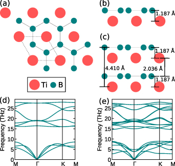
Figure 1. (a) Atomic structure of 2D-TiB2 with top view of nanosheets (monolayer (ML) and bilayer (BL)). Unit cell for the structures is highlighted in dashed frame. (b) Side view of ML is shown along-with the interlayer distance. (c) Side view of BL is shown along-with the relaxed and optimised distances between the different layers. Phonon dispersion curves along k-path M–Γ–K–M for (d) ML and (e) BL 2D-TiB2 nanosheets. Absence of imaginary frequencies indicates the dynamical stability of ML and BL 2D-TiB2 nanosheets.
Download figure:
Standard image High-resolution image4.1. Stability of 2D nanosheets
4.1.1. Structural model and stability.
TiB2 crystallises in the P6/mmm space group. We have studied 2D TiB2 ML and BL oriented in the (0001) direction. Ti atom is bonded in a six-coordinate geometry to six equivalent B atoms with all Ti–B bond lengths,  Å. Boron atom (B) is bonded in a six-coordinate geometry to three equivalent Ti and three equivalent B atoms. All B–B bond lengths,
  Å, which is in good agreement with previous findings (
 Å [31]). One unit cell of a single-layer contains two B atoms and one Ti atom, where the B atoms are arranged in a honeycomb lattice, and Ti atoms are located in the middle of the hexagons, as shown in figure 1. Further the structures for both ML and BL were relaxed, with optimised lattice parameters (lattice constants and layer thickness) and wyckoff sites listed in table 1. We also consider the different stacking configurations (AA and AB) for BL formation and found AB stacked BL to be dynamically and thermodynamically unstable due to presence of imaginary frequencies around Γ point in phonon dispersions and large energy fluctuations in AIMD calculations (see supplementary material), while AA stacked BL is found to be robust and stable. Hence in present study we use BL for AA stacked configuration of BL. In figures 1(a)–(c) we have shown structural arrangement of nanosheets (top and side views) with optimised interlayer separations. The equilibrium lattice constants of 2D-TiB2 nanosheets are
  Å which is comparable to previously reported results [29, 69]. Further structural robustness of nanosheets (ML and BL) was confirmed with the help of mechanical stability criteria (
 ,
,  ) as discussed in section 4.1.3.
Table 1. Relaxed and optimised lattice constant (a), layer thickness (h), wyckoff positions and corresponding coordinates of different atoms for 2D-TiB2 monolayer (ML) and bilayer (BL).
| a (Å) | h (Å) | Atom | Wyckoff position | x | y | z | |
|---|---|---|---|---|---|---|---|
| ML | 3.035 | 1.187 | Ti | 1a | 0.000 | 0.000 | 0.000 |
| B1 | 2b | 0.667 | 0.333 | 0.081 | |||
| B2 | 2b | 0.333 | 0.667 | 0.081 | |||
| BL | 3.035 | 4.410 | Ti1 | 1a | 0.000 | 0.000 | 0.000 |
| Ti2 | 1a | 0.000 | 0.000 | 0.220 | |||
| B1 | 2b | 0.667 | 0.333 | 0.081 | |||
| B2 | 2b | 0.333 | 0.667 | 0.081 | |||
| B3 | 2b | 0.667 | 0.333 | 0.301 | |||
| B4 | 2b | 0.333 | 0.667 | 0.301 |
4.1.2. Lattice, dynamical, and thermodynamical stability.
To study the lattice stability, we have plotted phonon dispersions along k-path M–Γ–K–M as shown in figures 1(d) and (e) for ML and BL, respectively. The absence of the imaginary frequencies reveals the dynamical stability of the 2D-TiB2 nanosheets. The maximum frequency of the acoustic branch of BL (8.86 THz) is higher than that of the ML (8.54 THz) which can be possibly attributed to the smaller restoring force of atomic out-of-plane vibrations in ML. This can lead to the higher Debye temperatures and increased bond-stiffness in BL as compared to ML. In figure 2 we have compared the atom-projected phonon density of states (pDoS) for ML and BL. Due to the significant differences in atomic weights of Ti and B atoms, a large phonon frequency bandgap exists in 2D-TiB2 nanosheets. We report the phonon frequency bandgap of 7.73 THz and 5.79 THz for ML and BL, respectively. The scattering between the acoustic and optical phonon modes can become forbidden with the increase in the phononic bandgap, which is evidently more pronounced in ML than in the BL. As evident from pDoS (figure 2), it can be concluded that the contributions to the acoustic modes in both ML and BL comes predominantly from Ti atoms, however, the optical modes are majorily contributed by the presence of the B atoms. To further study the thermodynamical stability we have performed the AIMD calculations at room temperature (300 K) for ML and BL (see supplementary material) and found energy fluctuations to be minimised indicating thermodynamical stability of 2D-TiB2 nanosheets.
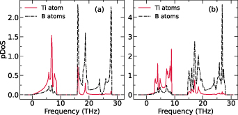
Figure 2. Phonon density of states (pDoS) for (a) monolayer (ML) and (b) bilayer (BL) 2D-TiB2 nanosheets.
Download figure:
Standard image High-resolution image4.1.3. Mechanical stability, properties and bonding Character.
The elastic properties of the 2D-TiB2 nanosheets are discussed in this section. Mechanical and elastic parameters for 2D-TiB2 nanosheets (ML and BL) calculated in applied strain range of 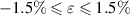 are reported in table 2. ML and BL satisfies the stability criteria as defined in section 2.1. Eigenvalues (
 ) of the stiffness matrix (in N m−1) for ML are 97.027, 147.779, and 194.053 while for BL are 127.318, 254.636, and 399.882. The positive eigen values of stiffness matrix for both ML and BL indicates their stable nature. In table 2, we compared the independent elastic constants, modulii, and ratios for ML and BL. In-plane stiffness (Young's modulus E) for 2D layers provides a measure of rigidity under the application of external load. We observe that with an increase in single layer (from ML to BL), the in-plane stiffness almost doubles (see table 2). Graphene has the highest stiffness among 2D materials (340 ± 50 Nm−1 [70]) owing to the presence of C–C bonds. The cumulative effect of presence of the additional layer (in BL) and slightly weakened bond strength due to the electron deficient nature of boron compared to carbon, explains the enhanced stiffness of 2D-TiB2 BL, approaching the stiffness values for graphene [70]. Such nature of boron bonding can also possibly explain the reduced in-plane stiffness of ML in comparison to graphene. In-plane elastic parameters (elastic modulii E and G and Poisson's ratio νxy
) for 2D-TiB2 nanosheets are highly isotropic in nature (see figure S1 in supplementary material). Poisson's ratio (ν) can be realised as a material's response towards the externally exerted stress on it. Mechanically stable 2D systems have ν between −1 and 0.5. Our calculated ν values for ML and BL (see table 2) falls in the range, indicating the mechanical stability of nanosheets.
) of the stiffness matrix (in N m−1) for ML are 97.027, 147.779, and 194.053 while for BL are 127.318, 254.636, and 399.882. The positive eigen values of stiffness matrix for both ML and BL indicates their stable nature. In table 2, we compared the independent elastic constants, modulii, and ratios for ML and BL. In-plane stiffness (Young's modulus E) for 2D layers provides a measure of rigidity under the application of external load. We observe that with an increase in single layer (from ML to BL), the in-plane stiffness almost doubles (see table 2). Graphene has the highest stiffness among 2D materials (340 ± 50 Nm−1 [70]) owing to the presence of C–C bonds. The cumulative effect of presence of the additional layer (in BL) and slightly weakened bond strength due to the electron deficient nature of boron compared to carbon, explains the enhanced stiffness of 2D-TiB2 BL, approaching the stiffness values for graphene [70]. Such nature of boron bonding can also possibly explain the reduced in-plane stiffness of ML in comparison to graphene. In-plane elastic parameters (elastic modulii E and G and Poisson's ratio νxy
) for 2D-TiB2 nanosheets are highly isotropic in nature (see figure S1 in supplementary material). Poisson's ratio (ν) can be realised as a material's response towards the externally exerted stress on it. Mechanically stable 2D systems have ν between −1 and 0.5. Our calculated ν values for ML and BL (see table 2) falls in the range, indicating the mechanical stability of nanosheets.
Table 2. Independent elastic Stiffness Constants Cij
(in N m−1), two-dimensional (2D) elastic modulii (Young's modulus E, Shear modulus G, and bulk modulus B, all in N m−1 units), and elastic ratios (in-plane Poisson's ratio νxy
and Pugh's  ratio) for monolayer (ML) and bilayer (BL) 2D-TiB2 nanosheets.
| C11 (N m−1) | C12 (N m−1) | E (N m−1) | G (N m−1) | B (N m−1) | νxy |

| |
|---|---|---|---|---|---|---|---|
| ML | 170.916 | −23.137 | 167.784 | 97.027 | 73.890 | −0.135 | 1.313 |
| BL | 327.259 | 72.623 | 311.143 | 127.318 | 199.941 | 0.222 | 0.637 |
The presence of the auxetic behaviour (negative Poisson's ratio NPR, see table 2) in ML is reported earlier [68]. Auxetic behaviour is generally observed in engineered bulk structures and is rare to sight in 2D materials [68, 71]. It is further shown that the addition of any extra layer (BL) destroys the auxetic behaviour (ν = 0.222) of freestanding 2D nanosheet. Such behaviour is mainly attributed to the presence of interlayer interactions in BL (and beyond) resulting in enhanced stiffness and non-auxetic behaviour. The increase in the Poisson's ratio (from negative to positive) can be fundamentally correlated to enhancement of in-plane stiffness in multilayer nanosheets. Distinct behaviour of Poisson's ratio for differently layered structures can also be attributed to the spatial constraints (in z-direction), where buckling height can be adjusted in multilayered systems while same cannot be realised in ML. Such behaviour is loosely based on atomic potential repulsion. The known 2D auxetic materials shows either in-plane NPR [72–79] or out of plane NPR [80–86], attributing to their re-entrant or hinged geometric structures [68, 87]. NPR cannot be attributed solely to geometry as both auxetic and non-auxetic behaviour is found in similar crystal structure for differently layered systems. Recently Yu et al showed that the auxetic behaviour of the materials could also be determined by their distinct electronic structures [87]. We have further investigated the distinct electronic structures of ML and BL (as discussed in section 4.2), which can possibly explain the origin of NPR in ML (in addition to structural features) and absence of auxetic behaviour beyond single layer of 2D-TiB2. The strong coupling between d orbitals (Ti-atom) and pz orbital (B-atoms) can possibly attribute for auxetic behaviour in ML [68].
Additionally, the brittle-ductile behaviour and bonding nature is studied by constraining  ratio and in-plane poisson ratio νxy
inline with the Pugh's [88] and Frantsevich [89] criteria. Transition between the brittle and ductile nature happens at
ratio and in-plane poisson ratio νxy
inline with the Pugh's [88] and Frantsevich [89] criteria. Transition between the brittle and ductile nature happens at  (Pugh's criteria [88]), where materials having
  behaves in a ductile manner while those with
  shows brittle nature. Our results (presented in table 2) indicates that both ML and BL are brittle in nature, however the brittleness has been drastically reduced by addition of a single layer.
  ratio for BL has remained less than half of the value for ML (table 2). Hence, such addition of multiple layers can be perceived as engineering parameter to change the behaviour from brittle to ductile nature. Also, constraining ν value at 0.26 (Frantsevich criteria [89]) provides additional insights into the brittle–ductile nature, where ν < 0.26 indicates brittle nature and for ν > 0.26 favours ductile nature. Based on constraining of ν value, both ML and BL are brittle in nature, while it is evidently seen in our calculations (table 2) that BL makes significant transition towards the ductile nature from the brittle behaviour of ML.
Further the bonding character of nanosheets is studied based on the Pettifor's criterion [90, 91], where positive (negative) Cauchy pressure indicates intrinsically ductile (brittle) nature attributed to non-directional metallic (directional covalent) bonds. Analogically to cubic crystals, in our present study for 2D isotropic hexagonal systems, we define Cauchy pressure as  . Hence we report CP for ML and BL as −120.164 and −54.695 N m−1, respectively. It is evident that both ML and BL contains directional covalent bonds while being intrinsically brittle in nature where brittleness of BL is drastically reduced as compared to ML. The bonding character is also studied based on the electron localisation function (ELF) as discussed in section 4.2.
For application-based needs and experimental feasibility, free-standing ML needs to be stabilised on a substrate (h-BN [31], hexagonal MoS2 [68]) to avoid its bending tendency [31, 92]. It is however recently shown that TiB2 derived nanosheets can also act as cement additives to enhance stabilisation and hydration properties of C2S [93].
4.2. Electronic properties
Subsequently, we investigated electronic properties of ML and BL to study the origin of observed properties and interdependence of electronic structure on the optical properties. To extend the study of bonding character of nanosheets, we have calculated the ELF for ML and BL (see ELF maps for ML and BL at figure S2 in supplementary material). The B–B bonds are of covalent character owing to presence of localised electrons, however the strong localisation around small region in vicinity of metal atoms indicates the electron transfer from metal to electron deficient boron atoms, which helps in stabilising the nanosheets. ELF indicates that bonding in nanosheets is predominantly of covalent nature.
We further studied the band structure of the ML and BL using PBE functional and ultrasoft pseudopotentials along the K-path Γ–M
 –Γ. Dirac cone at the fermi level have been previously reported for ML [31], while we report the metallic kind of band structure for BL where few conduction and valence bands cross the fermi level. Band structure for both ML and BL are compared in figure 3, where contributions from atomic orbitals (Ti and B orbitals) is projected onto the band structure. Projected band structure suggests that near the fermi level major contributions are from Ti(d) and B(p) orbitals. Several dispersive (not flat) bands cross fermi level of BL, which are predominantly contributed by the Ti(
 ) and B(pz
and traces of px
) orbitals. We further examined the effect of SOC on the band structures (see figures S3 and S4 in the supplementary material), to find that a bandgap of 0.057 eV is introduced in ML along with the small spin splitting of bands for both ML and BL. The in-plane (Sx
and Sy
) contributions of spin is much pronounced compared to the z-component. We also plotted three-dimensional valence highest occupied molecular orbital (HOMO) and conduction lowest unoccupied molecular orbital (LUMO) bands (see figure 4) to study band contours and the dispersive nature. In figures 4(b) and (d), we have shown contour plots at the fermi level for ML and BL, respectively. The contour plot for BL clearly shows the anisotropic and dispersive nature of bands crossing the fermi level, while contour plot for ML shows the formation of dirac cones with anisotropic nature in agreement with previously reported findings [31]. In their recent work, Abidi and Koskinen [94] have studied the effect of different pure and hybrid exchange-correlation functionals for low-dimensional (specifically 2D) metallic systems. In their work they have optimised that HSE06 is the best and robust hybrid functional to work with 2D metallic systems followed by HSE03, PBE, and others. Hence to overcome the underestimations using PBE functional, we performed the band structure calculations of ML and BL TiB2 nanosheets more accurately using hybrid HSE06 functional (see supplementary material). HSE06 indeed opens up a small amount of direct bandgap (0.115 eV) at Dirac point in ML, while the BL retains its metallic nature.
) and B(pz
and traces of px
) orbitals. We further examined the effect of SOC on the band structures (see figures S3 and S4 in the supplementary material), to find that a bandgap of 0.057 eV is introduced in ML along with the small spin splitting of bands for both ML and BL. The in-plane (Sx
and Sy
) contributions of spin is much pronounced compared to the z-component. We also plotted three-dimensional valence highest occupied molecular orbital (HOMO) and conduction lowest unoccupied molecular orbital (LUMO) bands (see figure 4) to study band contours and the dispersive nature. In figures 4(b) and (d), we have shown contour plots at the fermi level for ML and BL, respectively. The contour plot for BL clearly shows the anisotropic and dispersive nature of bands crossing the fermi level, while contour plot for ML shows the formation of dirac cones with anisotropic nature in agreement with previously reported findings [31]. In their recent work, Abidi and Koskinen [94] have studied the effect of different pure and hybrid exchange-correlation functionals for low-dimensional (specifically 2D) metallic systems. In their work they have optimised that HSE06 is the best and robust hybrid functional to work with 2D metallic systems followed by HSE03, PBE, and others. Hence to overcome the underestimations using PBE functional, we performed the band structure calculations of ML and BL TiB2 nanosheets more accurately using hybrid HSE06 functional (see supplementary material). HSE06 indeed opens up a small amount of direct bandgap (0.115 eV) at Dirac point in ML, while the BL retains its metallic nature.
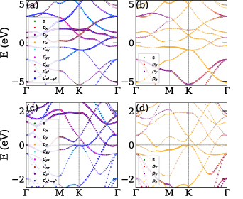
Figure 3. Band structure of 2D-TiB2 nanosheets along the k-path Γ–M–K–Γ with orbitals projections on the bands. Projection of (a) titanium (Ti) orbitals and (b) boron (B) orbitals on the band structure of monolayer 2D-TiB2 nanosheet depicting major contributions from Ti d-orbitals and B p-orbitals near the fermi level. Band structure for bilayer 2D-TiB2 nanosheet with projection from (c) titanium (Ti) orbitals and (d) boron (B) orbitals, revealing the contributions from Ti d-orbitals and B p-orbitals. The Fermi level is set to 0 eV.
Download figure:
Standard image High-resolution image
Figure 4. Three dimensional band-structure of HOMO and LUMO bands for monolayer (ML) and bilayer (BL) 2D-TiB2 nanosheets. (a) and (c) Shows the highest valence and lowest conduction bands for ML and BL, respectively. Bands for ML depicts the formation of six dirac cones at the fermi level, while BL bands shows the dispersive band nature at the fermi level which hints at its metallic nature. (b) and (d) Shows the contour plot at the fermi level for ML and BL, respectively. Contour plot for ML shows the formation of dirac cones with anisotropic nature, while for BL it depicts the highly anisotropic band structures.
Download figure:
Standard image High-resolution imageWe observe that the band nature changes from linear to dispersive with addition of single extra layer in ML, such that BL does not host any Dirac fermions with bands crossing the fermi level. To understand the changes in band nature, we probed ML by artificially varying the distance between the boron and titanium atoms starting from the relaxed parameter (h = 1.187 Å) with integral increment of 0.01 Å (see table 3). It is interesting to observe that with the increase in distance between titanium and boron layers, linear valence band crosses the fermi level (at titanium and boron interlayer distance of 1.32 Å, see table 3 and figure S5(k) in supplementary material) changing the nature of ML to metallic from a zero gap dirac material. It is evident from table 3 that upto the separation of 1.31 Å, dirac state in ML is nearly zero (narrow) gap with the gap in  eV. Using parabolic fitting of the band edges, the effective mass of the charge carriers (holes and electrons in highest valence and lowest conduction band, respectively) is calculated till the bands cross the fermi level and is presented in table 3 for two distinct paths towards Γ and K point from the dirac point (
![$D = [0.14, 0.14, 0.00]$](https://content.cld.iop.org/journals/0953-8984/36/4/045501/revision3/cmad0353ieqn86.gif) ) of ML in the reciprocal space. It is clearly seen that D–Γ is the preferred direction of electron motion. Owing to the lower effective mass values for ML, it can be utilised for high-bandwidth applications [95]. Electronic structure also helps in unravelling the fundamentals for vanished auxetic behaviour with addition of single extra layer in ML (in case of BL). Further mechanical calculations for artificially achieved metallic state of ML reveals the NPR for metallic state, which clearly indicates that simply the crossing of fermi level by linear electronic band (metallic behaviour) does not destroy the auxetic behaviour. The presence of several bands crossing the fermi level in BL can be fundamentally correlated to the enhanced in-plane stiffness and hence positive Poisson's ratio.
) of ML in the reciprocal space. It is clearly seen that D–Γ is the preferred direction of electron motion. Owing to the lower effective mass values for ML, it can be utilised for high-bandwidth applications [95]. Electronic structure also helps in unravelling the fundamentals for vanished auxetic behaviour with addition of single extra layer in ML (in case of BL). Further mechanical calculations for artificially achieved metallic state of ML reveals the NPR for metallic state, which clearly indicates that simply the crossing of fermi level by linear electronic band (metallic behaviour) does not destroy the auxetic behaviour. The presence of several bands crossing the fermi level in BL can be fundamentally correlated to the enhanced in-plane stiffness and hence positive Poisson's ratio.
Table 3. Electronic parameters of band structures along high-symmetry path Γ–M–K–Γ for artificially probed layer thickness h (in Å) for monolayer (ML) TiB2. The system shows the metallic nature beyond the critical layer separation of 1.31 Å. D denotes the high-symmetry K-point [0.14, 0.14, 0.00] in the reciprocal space corresponding to the Dirac state of ML.  denotes the bandgap in units of eV, while
  and
and  denotes the effective mass of hole and electron, respectively.
| h |

|

|

|

|

|

|
|---|---|---|---|---|---|---|
| (Å) | Nature | (eV) | (D–Γ) | (D–K) | (D–Γ) | (D–K) |
| 1.187 | Direct | 0.002 | −0.020 | −0.022 | 0.023 | 0.019 |
| 1.19 | Direct | 0.001 | −0.020 | −0.023 | 0.022 | 0.020 |
| 1.20 | Direct | 0.007 | −0.022 | −0.022 | 0.026 | 0.019 |
| 1.21 | Direct | 0.004 | −0.020 | −0.024 | 0.022 | 0.021 |
| 1.22 | Direct | 0.004 | −0.021 | −0.022 | 0.024 | 0.020 |
| 1.23 | Direct | 0.007 | −0.020 | −0.025 | 0.022 | 0.022 |
| 1.24 | Direct | 0.001 | −0.021 | −0.022 | 0.023 | 0.020 |
| 1.25 | Direct | 0.008 | −0.024 | −0.022 | 0.026 | 0.020 |
| 1.30 | Direct | 0.003 | −0.023 | −0.022 | 0.024 | 0.022 |
| 1.31 | Direct | 0.008 | −0.027 | −0.022 | 0.026 | 0.022 |
| 1.32 | Metallic | — | — | — | — | — |
| 1.33 | Metallic | — | — | — | — | — |
| 1.34 | Metallic | — | — | — | — | — |
| 1.35 | Metallic | — | — | — | — | — |
| 1.40 | Metallic | — | — | — | — | — |
We have further calculated the fermi surface for BL and constant energy isosurfaces for ML at different chemical potentials (µ) in the range of 0 to 0.5 eV for both valence and conduction bands to evaluate the fermi velocity. Development of ML branches from µ = −0.5 to 0.5 eV and BL for µ = 0 eV is shown in figure S7 of supplementary material, in the reduced zone scheme. We find that the average velocities across the fermi surface for both BL and ML are in the order of 105 m s−1. BL being intrinsically metallic in nature, shows several signatures of nesting which can perhaps leads to the charge density wave (CDW) formation. Experimental tuning of the distance between titanium and boron layers is quite challenging, attributing to the strong metal–boron bonds. It is recently shown that by disrupting the stable boron–boron ring structure, hydrogen storage capacity of similar class of 2D metal boride MgB2 can be drastically increased [96], where partially exfoliated multilayers of MgB2 were produced by mechanochemical exfoliation in zirconia resulting in 3–4 nm thick MgB2 nanosheets [96]. Recent studies have developed various approaches to exfoliate TiB2 into nanosheets, which opens up the avenue for practical applications such as enhancing the CO2 capturing ability of CaO [36], enhancing the adsorption and activation of nitrogen [37], and as cement additives [93]. With such increased experimental footprints in budding novel direction for 2D metal borides, if we are able to control titanium and boron layers separation in TiB2 nanosheets, by suggestive means of intercalations or other suitable experimental approaches, it would be promising to utilise 2D TiB2 in device applications.
4.3. Optical properties
In 2D materials, excitonic effects plays an important role in correctly determining the optical activity, attributing to geometrical confinement and reduced Coulomb screening [97, 98]. To obtain reliable results, electron–hole interactions must be taken into consideration. In this last subsection, we will focus on the optical properties of the low-dimensional 2D nanosheets (ML and BL) of TiB2. Due to the strong depolarisation effect in 2D planar geometry for light polarisation perpendicular to the plane, the optical properties for light polarisation parallel to the plane are discussed.
The imaginary  part of the dielectric functions of ML and BL were calculated for the in-plane polarized directions as shown in figure 5. Both ML and BL shows better light absorption in NIR region, which is evident from the high absorption peaks (figure 5) at photon energies of approximately 0.16 eV (DFT), 0.82 eV (BSE) for ML and 0.12 eV (DFT), 1.01 eV (BSE) for BL. As shown in figure 5, small optical activity is also observed on the interface of IR and visible regions. Since majority component of natural light consists in visible and infrared regions, our findings suggest that such 2D materials are promising candidates for diverse optical, photocatalytic, and photovoltaic applications. The real
  part of the dielectric function at zero energies provides the static dielectric constants, which were calculated to be 47.62 and 26.70 for ML and BL, respectively (see figure S8 supplementary material). Variation of
  hints about the electronic polarisability of the nanosheets, indicating that with successive addition of layer, polarisability decreases.
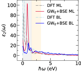
Figure 5. Imaginary part of the dielectric function  of 2D-TiB2 nanosheets (monolayer (ML), and bilayer (BL)), in a wide range of photon energies
  (in units of eV). Grey and orange shaded areas refers to the infrared (IR) and visible regions, respectively, while the unshaded (white) region refers to the ultraviolet energies.
Download figure:
Standard image High-resolution imageReal and imaginary parts of in-plane 2D optical conductivity for ML and BL (see figure S9 in supplementary material), provides insights about the optical response of the nanosheets in different regions (IR, visible, and UV). Based on the 2D optical conductivity, we further obtained optical spectra for ML and BL, at DFT (without the electron–hole interaction) and GW0-BSE (excitonic effects included) levels. Our results of absorption, transmission, and reflection spectra as a function of the photon energy, as depicted in figure 6, reveals that inclusion of excitonic effects slight modify the spectral peak positions. For both ML and BL, the excitonic absorption edges are slightly blue-shifted, with relative absorption intensity increased for ML and decreased for BL. The reflection tendency is very less as compared to absorption and transmission values. In figure 6, reflection and transmission values are appropriately scaled for visualisation, where the transmission spectra can be seen as negative spectrum for absorbance values. We have marked the highest absorption peaks for ML (as P1, P2, and P3) and BL (as 1, 2, *, 3, 4, 5, 6, 7, 8, 9, and 10) to observe the optical activity in different optical regions. As shown in figure 6, we find that including excitonic effects, ML show good ability to absorb light in the UV and NIR regions, which is evident from the high absorption peaks at approximately 0.86 (P1), 3.67 (P2), and 7.24 eV (P3). It is interesting to note that with the excitonic effects, while the relative intensities of the peaks have reduced in BL, optical activity has been increased upon addition of an extra layer (in BL as compared to ML) across wide range of photon energies spanning IR, visible, and UV regions, which is evident from relative intensities and peak positions (as 1, 2, *, 3, 4, 5, 6, 7, 8, 9, and 10 in figure 6). Excitonic effects plays an important role in optical activity of 2D materials, which is evident from appearance of optical peak (*) in the visible region of BL (figure 6(d)), which can be regarded as the excitonic peak in BL. The optical activity across wide range of energies in BL can be attributed to the presence of several dispersive bands crossing the fermi level in BL as compared to the presence of linearly dispersive dirac cone in ML. Such distinct band nature of ML and BL near the fermi level is believed to be the reason for varied optical activity of differently layered nanosheets.
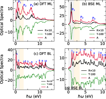
Figure 6. Optical properties: reflection  10 (black solid line), transmission
  (green dashed line), and absorption
  (red solid line) for (a) and (b) monolayer (ML) and (c) and (d) bilayer (BL) 2D-TiB2, as a function of photon energies
  (in units of eV) under the assumption of normal incidence. Grey and orange shaded areas refers to the infrared (IR) and visible regions, respectively, while the unshaded (white) region refers to the ultraviolet (UV) energies. The scaling of reflection
  and transmission
  is considered for visualisation. The prominent absorption
  peaks (marked in blue color) for monolayer and bilayer are identified as P1, P2, P3 and 1, 2, *, 3, 4, 5, 6, 7, 8, 9, 10, respectively, across wide range of photon energies
  (in units of eV) spanning IR, visible, and UV regions.
Download figure:
Standard image High-resolution imageTo further examine the dependence of optical activity on the electronic structure, we have calculated the transition probabilities from the highest valence to the lowest conduction bands for ML. The transition probability for ML at the off-symmetry dirac point has high values of the order of 104 Debye2 (see figure 7), however including the SOC effects we observed that the transition probabilities span an area between the high symmetry M and K points in the order of 108 Debye2 because the energy is no longer strictly proportional to the wave vector. BL contains several bands crossing the fermi level, while we have calculated the transition probabilities between band indexes 10 and 11 (see figure S6 in supplementary material) to observe that transition peaks exists at multiple points in k-space, which is in agreement with the observed optical activity across wide range of photon energies. It is further interesting to observe that transition probabilities for BL are of the order of 103 Debye2, which is significantly less than ML, and even SOC does not change the order of transition probabilities of BL which is in agreement with our spectral results. The high transition probabilities of ML can be accounted to the presence of the linear bands and Dirac channels as very less to no threshold energy is utilised to move the carrier electrons from occupied to unoccupied states, which is further tunable by spintronic effects (such as SOC). Enhancement of transition probabilities with SOC can pave the way for spintronic applications. Finally, the enhanced optical activity of ML in infrared and ultraviolet regions can be attributed to splitting of linear bands regulated by spintronic effects which introduces small gap of 0.057 eV in ML. Further HSE06 calculations opens up direct gap (0.115 eV) at dirac point in ML accompanied by high transition probabilities, which can be attributed for sharp peaks in IR and UV regions. Also, the electronic polarisability of BL is reduced compared to ML which can be correlated with the decreased optical activity of BL. The metallic nature BL (at PBE and HSE06 levels) can also restricts its absorbance tendency which explains the reduced optical activity in NIR and UV regions. Being optically active in IR and UV regions, ML can be utilised for ultrafast photonic applications accounting to high values of transition probabilities, and BL being optically active in wide energy range can be utilised for device applications in broad regions of interest.

Figure 7. PBE calculated band structure (top panel) and transition probabilities P2 (bottom panel, in units of Debye2) for monolayer ML 2D-TiB2 (a) without and (b) with spin–orbital coupling (SOC) effects. Without SOC transition peak appears at the off-symmetry Dirac point marked by the green (dashed line) vertical.
Download figure:
Standard image High-resolution image
5. Conclusion
In conclusion, by combining phonon-dispersions, molecular dynamics and mechanical calculations, we show that 2D-TiB2 nanosheets (ML and BL) are mechanically, thermodynamically and dynamically stable. The absence of the negative frequencies in the phonon dispersion curves indicates the dynamical stability of the nanosheets with much higher phonon bandgap in ML (7.73 THz) compared to that of BL (5.79 THz). Small temporal energy fluctuations at room temperature indicates the thermodynamic stability of 2D-TiB2 nanosheets. Our findings reveal that the addition of any extra layer (as in BL) destroys the auxetic behaviour (ν increases from −0.135 for ML to 0.222 for BL), which can be fundamentally correlated to increased bond stiffness (in-plane) in BL (almost doubles compared to ML). Constraining Pugh's G/B ratio and in-plane poisson ratio reveal that both ML and BL are brittle in nature, however the brittleness has been drastically reduced by addition of a single layer. We find that SOC causes small spin splitting of bands for both ML and BL, while it introduces small gap of 0.057 eV in ML. Also, HSE06 functional opens up a small amount of direct bandgap (0.115 eV) at dirac point in ML, which can be attributed for increased optical activity of ML compared to BL. In addition, we find that with the increase in distance between titanium and boron layers, linear valence band crosses the fermi level (at titanium and boron interlayer distance of 1.32 Å) forming a low-dimensional metallic state of ML. Furthermore, mechanical calculations for metallic state of ML reveal that the crossing of fermi level by linear electronic band (metallic nature) does not destroys the auxetic behaviour of ML. We further find that with successive addition of layer, electronic polarisability of the nanosheet decreases. The calculations of optical spectra as a function of the photon energy (based on 2D optical conductivity) reveal that excitonic effects (electron–hole interactions) induces the slight blue-shift of the DFT calculated absorption spectra for both ML and BL, where ML is optically active with sharp peaks in IR and UV regions while BL shows the reduced optical activity across wide range of photon energies spanning the NIR to UV region. Furthermore, the calculations show high transition probabilities of ML at Dirac point which are tunable by spintronic effects (SOC). Thus, our findings suggest that ML and BL 2D-TiB2 nanosheets have great potential for utilisation in variety of optoelectronic and spintronic applications.
Acknowledgment
We are thankful to Department of Physics, Himachal Pradesh University for the logistic support. A T acknowledges support received from the Purdue School of Engineering and Technology, IUPUI.
Data availability statement
The data that support the findings of this study cannot be made publicly available because it forms the part of the ongoing research. However, it is available upon reasonable request from corresponding author. The data that support the findings of this study are available upon reasonable request from the authors.
Conflict of interest
The authors declare that they have no known competing financial interests or personal relationships that could have appeared to influence the work reported in this paper.
Supplementary data (4.4 MB PDF)