

Abstract
Quantum electronics has significantly evolved over the last decades. Where initially the clear focus was on light–matter interactions, nowadays approaches based on the electron's wave nature have solidified themselves as additional focus areas. This development is largely driven by continuous advances in electron quantum optics, electron based quantum information processing, electronic materials, and nanoelectronic devices and systems. The pace of research in all of these areas is astonishing and is accompanied by substantial theoretical and experimental advancements. What is particularly exciting is the fact that the computational methods, together with broadly available large-scale computing resources, have matured to such a degree so as to be essential enabling technologies themselves. These methods allow to predict, analyze, and design not only individual physical processes but also entire devices and systems, which would otherwise be very challenging or sometimes even out of reach with conventional experimental capabilities. This review is thus a testament to the increasingly towering importance of computational methods for advancing the expanding field of quantum electronics. To that end, computational aspects of a representative selection of recent research in quantum electronics are highlighted where a major focus is on the electron's wave nature. By categorizing the research into concrete technological applications, researchers and engineers will be able to use this review as a source for inspiration regarding problem-specific computational methods.
Export citation and abstract BibTeX RIS

Original content from this work may be used under the terms of the Creative Commons Attribution 4.0 licence. Any further distribution of this work must maintain attribution to the author(s) and the title of the work, journal citation and DOI.
1. Introduction
The field of quantum electronics was originally established based on the developments of the microwave/light amplification by stimulated emission of radiation (MASER/LASER) principle 3 [1, 2]. However, looking at the broader electronics research today and considering that quantum is synonymous with wave or wave nature, there is a wide variety of areas in which electrons are treated as waves, e.g., [3–10]: we thus conclude that quantum electronics has broadened its topical coverage. This can be seen, in particular, in the confinement-centric area of nanoelectronics, where quantum effects are to a large degree detrimental, and in solid-state quantum information processing approaches, where the wave nature of electrons is the core property needed for realizing the desired operations. Let us look more closely at these two highlighted areas; in-depth discussions are provided in the later sections.
The astonishing advances towards next generation electronic technologies continue to translate into miniaturization to further increase integration densities. This can clearly be seen by the staggering feature scale reductions over time and the plethora of research efforts to advance nanoelectronic devices and systems. 4 Many new technologies are being investigated among which are novel device designs (e.g., gate-all-around (GAA) nanosheet/nanoribbon field-effect transistors (FETs)), operational conditions (e.g., cryogenics, superconducting approaches), logic approaches (e.g., charge or non-charge), and materials (e.g., two-dimensional (2D) materials). Owing to continued miniaturization, these developments go hand in hand with highly confined device designs. Confinement of course introduces quantum effects in the electron transport owed to the wave nature of electrons. From a computational perspective, quantum models are then required to properly describe the electron behavior 5 .
Other efforts to develop next-generation electronic platforms focused on advancing towards the single-electron regime. First steps were made over 30 years ago with single-electron electronics [12] which materialized along the single-electron tunneling transistor [13] and the single-electron source [14]. In 2007, yet another important step was made, the realization of an on-demand coherent single-electron source [15]: it was now possible to generate electrons with well-defined wave-functions. This ability together with coherent waveguides allowed to conduct wave-based experiments using electrons. Naturally, at the forefront were interference experiments, inspired by the optical world [16–19]. It is thus not surprising that the surrounding research area was coined electron quantum optics. These fascinating achievements spawned many other research avenues, among which are alternative solid-state quantum information processing approaches, named flying charge qubits, where the electron charge (instead of the normally considered electron spin) is used to encode a qubit [6]. Contrary to the previously discussed quantum effects in conventional nanoelectronic systems, where quantum effects tend to be detrimental, here the wave nature and the corresponding quantum effects are the core feature upon which the entire system operation relies. Considering a computational perspective and as with nanoelectronics, again quantum models are required to properly describe the electron behavior, such as, transport dynamics.
In all of the quantum electronics research areas experiments are of course essential to drive research forward. However, experimental considerations can be challenging in the quantum realm [20]. What is astonishing though, is the fact that in addition to conventional experiments and fueled by the prevalent ultra-confined systems in next-generation device designs, advances in computational methods matured to a degree where they exceeded their historical role as a side-tool (in many cases only usable by a select few experts, such as with electronic structure methods [10]) to support development. In fact, there are nowadays many cases where computational methods are the sole way to provide insights into the fundamental governing physical processes. One manifestation of this development is materials by design [21], collectively describing efforts for computationally designing materials ahead of potential realization in fabrication facilities. Of course, software requires hardware to actually be executed. Due to the tremendous advancements of microelectronics large-scale computing resources are broadly available and allow for computational experiments of astonishing scale and scope.
Coming back to the computational methods, indeed many different methods are available providing a wealth of investigative opportunities. By way of example and as will be discussed later in more detail, consider electronic structure calculations via density functional theory (DFT) or an electron quantum transport simulation to compute the electron density within a driven device, or a combination of both.
To that end, this review highlights a selection of recent quantum electronics advances where computational methods were essential for the findings. The focus is (i) on research from the past roughly 3–4 years to provide an overview of very recent applications, and (ii) on research where electrons and their wave nature are at the center. We list for each contribution at least one of the applied core computational methods. This will allow researchers and engineers to quickly assess the computational landscape for each area of application. This will incentivise readers to consider new computational experiments and alternative computational methods.
1.1. What this review covers
Section 2 provides a short overview of the key computational methods identified in the research reviewed in the later sections. A particular focus is on the methods which are applied the most, such as for calculating the electronic structure and the electron quantum transport. However, we also discuss other, alternative methods which see considerable use. We do not express a preference of one method over the other but merely reflect the extent of use in the research presented in this work.
Section 3 represents the first of the review sections and covers the previously highlighted area of electron quantum optics and the flying charge qubit systems. The section starts off by discussing the principal enabling technology: single-electron sources. In particular, mesoscopic capacitors, electron pumps, surface acoustic waves (SAWs), levitons, and locally modulated quantum Hall edge state sources are covered. This is followed by a discussion of essential waveguides (which enable one to build coherent quantum circuits) and of electron transport dynamics. Finally, interferometers, a core focus of electron quantum optics, and tomography, spectroscopy, and detection methods are highlighted.
Section 4 provides an overview of computational research into quantum dots and the predominant approach for realizing quantum information processing: spin qubits. Although spin transport itself is not at the focus of this review, a few selected works are presented where the electron wave nature is of particular relevance.
Section 5 highlights research in superconducting junctions, in particular normal-superconductor interfaces. These interfaces are particularly relevant for Josephson junctions and superconducting qubits.
Section 6 delves into the particularly strong focus area of 2D materials and topological materials and systems. In addition, light–matter interaction effects in materials are highlighted as are combinations of materials in the form of heterostructures; the latter enable one to further tune material properties. Finally, research into molecular junctions and systems is discussed, where typically a specific molecule (chain) is considered between contacts.
Section 7 provides an overview into research on next-generation FETs. The focus is of course on GAA designs, such as, nanoribbon FETs and 2D FETs. The latter further underlines the importance of 2D materials for nanoelectronic devices. The section is concluded by research on tunneling and other types of FETs, such as FinFETs and ultra-thin body FETs.
Section 8 discusses research on one of the core topics of quantum electronics, quantum cascade LASER (QCL) devices. To this day, research on QCL devices is a highly active field, particularly focusing on THz operation.
Finally, section 9 highlights research where electron transport is extended to include heat transfer into the electron transport modeling picture. Focus areas include illuminating fundamental transfer processes but also thermoelectric effects.
2. Computational methods
In this section we give an overview of computational methods typically used in computational quantum electronics and which were applied in the research presented in this review (see sections 3–9). To set the stage, we first discuss general issues concerning types of simulations and general theoretical considerations. We note that the method of many-body Green's functions can be used for both quantum transport and electronic structure simulations (i.e., in the form of the GW method, see section 2.4.2), which is why it is widely applied and we thus devote a separate section for an extended overview. We then summarize methods for electronic structure and quantum transport respectively as well as other, less used but still important methods.
This section is not meant to provide a detailed analysis of each method including a comparison but rather as a top-level overview of the methodological landscape. We refer to the individual extensive literature provided in the respective subsections for more details.
2.1. Simulation types
Simulations in quantum electronics can be broadly divided into simulations of electronic structures and quantum transport simulations. As indicated before, sometimes these simulations are combined, for instance, in an electronic structure simulation (e.g., using DFT) which is followed by a transport simulation (e.g., non-equilibrium Green's function (NEGF) approach). Many examples of such combinations are available and are discussed in the technological sections below.
Looking at the underlying simulation models, specification of models for quantum transport is complex, especially for realistic devices [22, 23]. The quantum mechanical states are coupled with the environment. The system is driven out of equilibrium by an applied bias. States get filled through the contact regions and through scattering interactions. Electrons interact with phonons over long distances. Some systems are highly inhomogeneous due to different materials used for active layers. Typically, parts of the nanosystem have reduced dimensionality. Proper open boundary conditions have to be applied and non-normalizable states have to be treated numerically. Because of the thus resulting modeling complexity, practical transport simulations often contain semi-empirical approximations. A typical system which is regularly considered in quantum electron transport consists in a nanosystem between electrodes.
2.2. Many-body interaction
Full inclusion of many-body interactions in the simulation is in general computationally intractable. To formulate computationally tractable models a closure problem has to be solved, which is discussed in the following after covering computational complexity.
2.2.1. Computational complexity
Models in computational quantum electronics are based in many-body quantum physics. We discuss computational costs using the example of a many-body model Hamiltonian describing electrons interacting through Coulomb force which is given in first quantization (in atomic units) as

Because the Coulomb interaction involves two electrons this problem cannot be reduced to a single-body problem. The electron wave-functions have domain  . If the problem is discretized using K grid points in
  the number of unknowns scales as KN
. A direct solution becomes computationally intractable already for low numbers N ∼ 10. However, often the system of interest consists of a large number of electrons or even worse one is interested in a limit N → ∞. Many computational methods work by effectively reducing the problem in some way to the case of independent particles.
the number of unknowns scales as KN
. A direct solution becomes computationally intractable already for low numbers N ∼ 10. However, often the system of interest consists of a large number of electrons or even worse one is interested in a limit N → ∞. Many computational methods work by effectively reducing the problem in some way to the case of independent particles.
2.2.2. The closure problem
On the highest level, models for quantum electronics are formulated in second quantization (Fock space) where spin and antisymmetry of the wave function are naturally included. If the underlying one-particle Hilbert space is modelled by a finite-dimensional Hilbert space with dimension K then the corresponding fermionic Fock space has dimension 2K . In realistic applications this is not numerically tractable and full knowledge of the many-body wave function is in general not possible.
A natural idea to extract information about the system is to solve for correlation functionals from which the observables of interest can be calculated. Physical observables are calculated as ensemble averages over the density operator 

Here the subscript H denotes the Heisenberg picture where the state is time-independent and the time dependence is carried by the operators. A striking example is charge density n(r) which is the basic quantity in DFT.
If two or more operators at (possibly) different times are involved the operator trace defines a correlation functional

However, formulating equations in terms of a few selected correlation functionals leads to a closure problem. Due to the interaction between particles the equations for a given fixed finite set of functionals will in general contain other functionals outside the fixed set and the resulting system is underdetermined (not closed). Closure problems emerge in many places in theoretical physics. We mention the closure problem for the BBGKY-hierarchy and solution methods for the Boltzmann equation, which try to reduce the distribution to a few of its moments. Hence, a useful way to classify models used in computational quantum electronics is the set of basic quantities (functionals) in which the theory is formulated together with a method of closure (see discussion of NEGF below).
For the sake of completeness, we note that in selected cases, such as the jellium model, an essentially exact calculation (i.e., without a closure) of specific ground-state functionals may be possible using quantum Monte Carlo methods [24, 25]. However, these methods are computationally far too expensive to use in all but the simplest cases [26].
2.3. Green's function methods
Green's functions are a general mathematical technique to derive explicit solutions to differential equations, see [27, 28] and especially [29]. Many-body Green's functions provide a powerful formalism as basically all models can be specified in terms of many-body Green's functions and second quantization.
Several of the calculation techniques in use for many-body Green's functions have been originally developed in quantum field theory [30, 31]. The classical text book by Kadanoff and Baym from 1962 [32] on Green's functions in and out of equilibrium has recently been republished in an annotated edition [33] which is highly recommended. Other early texts devoted especially to the application of Green's functions in solid state physics include [34, 35].
We want to mention that the full power of Green's functions is not always used, even if the method might be superficially denoted as NEGF. For example, the quantum transmitting boundary method (theoretically corresponding to a single-particle Schrödinger equation) [36] can be specified using a self-energy for the open boundary conditions in NEGF. Put differently, a simple model may still be specified in a powerful formalism.
2.3.1. One-particle Green's functions
A central role in second quantization is played by the field operators  ,
,  which annihilate/create a particle at location r. The Green's functions in statistical quantum mechanics are a linear combination of a small set of basic correlation functions involving the field operators. The simplest example is the single particle lesser Green's function

from which the electron density is calculated as [37, p 153]

Most expectation values of interest can be calculated from the knowledge of the basic Green's functions. Under steady-state conditions, the Green's functions depend only on the time difference τ = t − t'. The two-times Green's functions allow the study of time-dependent and time-nonlocal phenomena such as retarded interactions and memory.
2.3.2. Higher-order Green's functions
To illustrate the previously mentioned closure problem (section 2.2.2) in the case of Green's functions we discuss the equation of motion for the one-particle Green's function with Coulomb interaction v(r − r').
For the one-particle Green's function g(x, x') we get the equation [29, p 255]
where we used the shorthand x = (r, t) etc. Here,  denotes (r1, t1 + s) as s → 0+. The two-particle Green's function g2 entering above is defined as

with T the (fermionic) time-ordering operator. Therefore, in the presence of a pairwise interaction the equation of motion for the one-particle Green's function g involves the two-particle Green's function g2. The equation for the two-particle Green's function involves the three-particle Green's function and so on.
If an infinite number of higher-order Green's functions is included we see that the Green's function formalism reformulates the full problem. However, the attractiveness of the method is based on the fact that perturbative methods (Feynman diagrams [38]) can be used which allow the problem to be attacked in a systematic approximative way. We remark that the properties of the perturbation expansion are mostly unknown. The series might diverge or the convergence is only asymptotic [39].
2.3.3. Equilibrium Green's functions (Matsubara formalism)
At finite temperature under thermodynamic equilibrium the density operator  is given as

where we defined  with the number operator
  and β = 1/kB
T.
and β = 1/kB
T.
Time dependency is described by the operator  while an operator
  for real β is contained in the density operator. This observation motivates the study of the analytic continuation of Green's functions for imaginary time.
Important quantities, which can be calculated from the knowledge of the equilibrium one-particle Green's function, are the spectral density function, the density of states function, conductivity, and dielectricity (linear response functions). Peaks in the analytic continuation of the spectral function give rise to an interpretation as quasiparticles.
2.3.4. Nonequilibrium Green's functions (Keldysh formalism)
For the study of non-equilibrium phenomena the time-ordered Green's function formalism used in equilibrium is extended to the formalism of contour-ordered Green's functions.
The many-particle information about the system must be cast into various forms of self-energies which enter the equations of motion for the Green's functions. The interaction with the environment (e.g., scattering, open boundary conditions) is also included through self-energies and dissipative effects can be modeled.
The self-energy is rarely exactly known and in this way the closure problem emerges in NEGF quantum transport modelling. A valid approximation has to conserve macroscopic conservation laws. Typical approximations to the self-energy from electron–electron interaction like Hartree, Hartree–Fock, Born, T-matrix and the random phase approximation yield the conservation laws [40].
The reader is referred to text books for further information on applying the NEGF formalism to quantum electronics [4, 5, 24, 37, 41–43]. Furthermore, a pedagogical introduction to the theory of Green's functions in and out of equilibrium is provided in [44]. A mathematical account of Green's functions is presented in [45]. A review of NEGF for transient simulation is contained in [46]. Self-energy approximations are discussed in [47] which provides an overview on recent progress in the theory of NEGF. A critical view on using NEGF for nanoelectronic devices is given in [48]. Some representative examples of NEGF simulation tools are, e.g., Omen [49], NEMO5 [50], NESS [51], Atomistix [52], NanoTCAD ViDES [53], and Victory Atomistic [54].
2.4. Electronic structure methods
Electronic structure methods stem from the field of quantum chemistry and are used to calculate the ground-state properties of condensed systems, e.g., exact ground state density and energy. In the following, we provide a short overview of the key methods in this area. For a recent review of electronic structure methods see [10].
2.4.1. Density functional theory
DFT is a method to calculate the electronic structure of atoms, molecules, and solids. The method is highly popular as it appears to occupy a sweet spot in terms of trade off between quality of results and computational costs.
The basic unknown quantity in DFT is the one-particle observable n(r). Conceptually, DFT is a mean-field many-body theory of the ground state. The potential used in DFT is the sum of external potentials (determined by the elemental composition of the system) and an effective potential which represents the exchange–correlation energy (i.e., electron–electron interaction beyond mean-field; respecting the Pauli exclusion principle). Here, the closure problem (section 2.2.2) emerges in the form of the exchange–correlation potential VXC whose exact form is unknown. The effective single-particle potential can be written as

The ground state of this system has to be calculated in a self-consistent way which results in a non-linear system of equations coupling the one-particle wave functions.
DFT is sometimes referred to as the standard model for periodic solids [55]. Considering time-dependent DFT, there DFT is used for simulating electronic excitation processes [56]. Due to the popularity of the method the literature on DFT is extensive and without a claim of completeness, the reader is referred to textbooks, e.g., [57–62], and to reviews, e.g., [10, 63, 64]. Some examples for DFT simulation tools are, e.g., VASP [65], QuantumATK [66], DFTB+ [67], CP2K [68], Atomistix [52].
2.4.2. GW method
The letter 'G' in the name of the method denotes the Green's function formalism, whereas the letter 'W' denotes the screened Coulomb interaction. The GW method can systematically improve upon certain shortcomings of DFT-estimates [69]. The GW method requires an initial ground state solution which is usually calculated by the DFT method. The unknown exchange–correlation potential is replaced by a self-energy based on the random phase approximation [70]. However, the final GW result also depends on the exchange–correlation function chosen for the initial solution. For reviews of the GW method see [69–71].
2.4.3. Tight-binding
The tight-binding model is a semi-empirical approach used for calculating the electronic band structure. This approach assumes that interactions between atoms are localized and die off quickly with distance. Hence the kinetics can be modelled by a hopping process, where an electron can hop to one of its nearest neighbors [72]. The electronic wave function is a superposition of localized atomic orbitals [62]. The tight-binding model is closely related to the LCAO (linear combination of atomic orbitals) method commonly used in chemistry.
The tight-binding model is a non-sophisticated, one-electron model which can be routinely solved for even a very large number of atoms. As computational costs are much lower than for DFT it is preferentially used in conjunction with NEGF provided it is sufficiently accurate. A machine learning method for the parameterization of tight-binding Hamiltonians is presented in [73]. Exemplary simulation tools are KWANT [74], TKWANT [75], and NanoNET [76].
2.5. Transport methods
We consider here quantum transport methods which solve a transport equation to describe the electron transport within any kind of electronic device or system. Particularly challenging yet realistic scenarios include interactions with the environment via, for instance, contacts, phonons, or electromagnetic fields. In the following, we give an overview of the key full quantum transport methods which are capable of describing the wave nature of electrons. We thus omit semi-classical approaches. For in-depth discussions of quantum transport we refer the reader to standard text books, such as [3, 22, 23, 77–79] in addition to the text books mentioned in section 2.3.4. We remind the reader that the NEGF formalism is also used to describe electron transport. The corresponding discussion is provided in section 2.3 and thus NEGF is not further mentioned here.
2.5.1. Scattering matrix
The scattering-matrix (sometimes referred to as S-matrix) relates incoming and outgoing waves in a region. It enters quantum mechanics in the form of the Lippmann–Schwinger equation [80]. When this formalism is used for electron transport calculations it is often referred to as the Landauer–Büttiker approach. The basic idea of this approach is to describe (stationary) charge transport through a quantum conductor as a scattering process.
In the simplest case the scattering-matrix approach solely relies on basic properties of the scattering matrix (unitarity) and conserves charge and energy. Conductance is calculated from the transmission eigenvalues of the scattering matrix. This method is applicable as long as electrons traversing the structure experience only elastic scattering [81, ch 1.3]. However, the method can be generalized to inelastic processes by including the imaginary self-energy at the expense of a non-unitary S-matrix [5, ch 2.4.4].
The original Landauer formula, which applied to a system with two terminals (electron reservoirs), has been extended to multiple probes in the Landauer–Büttiker formula. If the two-terminal Landauer formula is construed as the quantum version of Ohm's law, then the Landauer–Büttiker formula contains both the quantum Ohm's law and the quantum Kirchhoff's law [72, 82]. The Landauer–Büttiker formula can also be justified by linear response theory (Kubo formalism), see [83]. The formalism includes the case when a magnetic field is present.
The scattering matrix approach can be applied to non-stationary quantum transport based on the Floquet theorem for the Schrödinger equation with a potential periodic in time [84]. Inelastic and decoherence effects in the Landauer picture are briefly reviewed in [85]. An application domain where the method is difficult to employ is single-molecule transport if electron–electron and electron–vibron interactions play an essential role, see the discussion in [86, p 216].
2.5.2. Master equations and reduced density operators
The quantum master equation approach deals with the irreversible dynamics of quantum systems coupled to a macroscopic environment. Equations are usually formulated for the one-time two-particles density function. When the degrees of freedom from the environment are traced out the effective description of the open system results in non-Markovian behaviour (memory effects). The transport operators for the reduced density become non-Hermitian incorporating dissipative effects. Textbooks describing the master equation approach include [87–89]. An introduction is given in [90].
2.5.3. Wigner function
Historically, the Wigner function has been introduced for the analysis of quantum corrections to classical stochastic mechanics [91] and thus has been derived from operator mechanics. Later the Wigner function formalism was established as an independent formulation of quantum mechanics based on the Moyal bracket and the star-product, which is denoted as quantum mechanics in phase space [92–95].
The Wigner function is a real quasi-distribution in phase space [96]. The formalism transfers many concepts and notions from classical to quantum mechanics, such as the aforementioned phase space but also the distribution function and the way of calculating the physical average 

Here Aw denotes the Weyl transform of the classical observable A(x, p) and the Wigner function fw plays the role of the classical probability distribution fcl(x, p).
In contrast to the classical Boltzmann distribution the Wigner function may take on negative values which is interpreted as an indication of quantum effects. As the formalism is close to a classical phase-space description it allows for mixed quantum/semi-classical modelling.
Many applications of the Wigner function (also outside of the electronic scope) are demonstrated in monographs [5, 48, 97] and in recent reviews [7, 95]. Using a Wigner function approach transport can be analysed in terms of signed particles and stochastic jump processes, hence Monte Carlo methods may be employed for simulation (see [79] for a recent monograph on stochastic approaches to electron transport in micro- and nanostructures). More recent advancements concern, for example, an extension of the theoretical framework for Monte Carlo, accessible descriptions of general electromagnetic fields [98], handling of boundary conditions [99], and an operator splitting spectral method for a Wigner–Poisson system [100]. A 1D/2D signed-particle Wigner transport simulator is available via ViennaWD [101, 102]. For non-trivial interaction mechanisms a closure problem exists in the Wigner formalism [78, p 98]. Other very recent advances of Wigner function methods for electronics (and photonics, but not further discussed here) can be found in a recent special issue [103] and cover, among others, handling of boundary conditions [104–106] and modelling and solution approaches [107–113].
2.5.4. Schrödinger–Poisson
In the Schrödinger–Poisson equation electron–electron interaction is included by assuming that one electron interacts with the average background potential of all other electrons. This is the prototypical single-particle Hartree mean-field approximation. For many applications an approach based on Schrödinger–Poisson is sufficient, e.g., [3, 114–118].
2.6. Other methods
Here we collectively mention a few other methods which are also used by the community. Among the methods is the so-called wave function approach [119–121]. This is yet another method to study time-resolved quantum electronics. Another method is the single-electron approach which was proposed as an extension of the Landauer approach for time-dependent drive [122, 123]. Tensor networks can be used as representations of quantum many-body states based on their local entanglement structure [124, 125]. Bayesian formalism can be applied to simulate measurement backaction in an electron detection setting [126]. A program for calculating maximally-localised Wannier functions from a set of Bloch states is available by Wannier90 [127]. Neural networks can be used to predict transport properties of a quasi-one-dimensional (1D) tight-binding model with disordered on-site energies [128]. Finally, Bohmian mechanics can be used to describe electron quantum transport [20, 129, 130].
3. Electron quantum optics and flying charge qubits
The continued down-scaling of electronic devices driven by substantial technological advancements over the last decades naturally lead to the single-electron regime. As previously discussed, this development opened up the field of single-electron electronics [12], which, aside from introducing the single-electron tunneling transistor [13], also yielded the first single-electron sources, focusing on charge transfer [14]. Here we want to particularly highlight the role of the single-electron source, its development led to an important milestone: on-demand coherent single-electron sources [15]. The keyword coherent is essential here as the generated electrons have well-defined wave-functions (e.g., Gaussian [131]), enabling one to engineer coherent manipulations of electrons similar to the optical world. Having access to reliably generating individual coherent electrons opened up a new field of research focusing on the wave nature of electrons, electron quantum optics, which in turn facilitated a new research branch focusing on flying charge qubits for solid-state quantum information processing. For reviews on both areas see, e.g., [6, 132]. In addition, these developments were accompanied by research into waveguides, electron transport dynamics, interferometers, as well as tomography, spectroscopy, and detection methods.
3.1. Single-electron sources
As indicated before, a major milestone for coherent electronics was the development of coherent single-electron sources. In essence, three different approaches emerged: the first is based on the discrete level spectrum or Coulomb blockade effect in strongly confined systems. Realizations have been made via mesoscopic capacitors in the quantum Hall regime (e.g., [15]), superconducting turnstiles (e.g., [133]), electron pumps (e.g., [134]), and sound waves (e.g., [135]). The second uses Lorentzian-shaped voltage pulses to generate so-called levitons (e.g., [136]). And the third approach utilizes the local gate modulation of a quantum Hall edge state for noiseless single-particle emission on top of the Fermi sea (e.g., [137]). The review of Bäuerle et al provides an excellent overview of different single-electron source technologies [6]. In what follows, we highlight recent work in these areas, underlining the highly active field of research.
3.1.1. Mesoscopic capacitors
Mesoscopic capacitors have been around since many decades [138–140]. In particular, Fève et al applied the mesoscopic capacitor concept in 2007 to implement an on-demand coherent single-electron source by periodically driving a quantum dot [15]. In essence, the approach is based on driving an RC circuit by alternating-current (AC) voltage so as to limit the charge and discharge of the capacitor to a single elementary charge. The generated electron and hole is then emitted into a ballistic quantum Hall channel.
Selection of recent computational research: Yin used a scattering matrix approach to introduce a general method to extract the wave function of quasi-particles (i.e., electrons and/or holes in the Fermi sea) [141]. The excitation probability and the one-body wave function can be derived from the scattering matrix. The author used the approach to compare the characteristics of sources based on quantum dots and on an alternative approach based on quantum point contacts, showing clear differences in the differently generated particle features.
Wagner et al introduced a theoretical model of a single-particle emitter of charge pulses that uses a quantum dot coupled to a quantum Hall edge state by using a generalized master equation approach [142]. The authors used the model to highlight the Coulomb interactions between the dot and the chiral quantum Hall edge caused a destruction of precise charge quantization in the emitted wave packet. The research thus questions the viability of this particular setup as a single-electron source of quantized charge pulses.
Gurvitz used the single-electron approach to investigate the time-dependent electron current through a quantum dot under external drive, which is coupled to leads at zero bias (one lead as in the case of single-electron sources) [123]. A simplified formula describing the time-dependent current through the quantum dot is derived and investigated by using different driving pulse shapes. It was found that the current is indeed time-dependent at steady-state, but is zero if averaged over a time period for any external drive.
Particularly interesting work focuses on extending the work of single-electron sources to multi-electron sources. Such multi-electron sources would enable entirely new experiments and applications, such as quantum tomography (section 3.4) protocols. Based on previous work (e.g., [143]), in [144], Moskalets et al used Floquet scattering theory to describe composite two-particle sources composed of several single-particle emitters connected in series to a chiral waveguide in the (non-)adiabatic regime, see figure 1. The flexible design allows for more than two sources and for mixing source types, such as mixing a leviton source (section 3.1.4) with a mesoscopic capacitor. In follow up work, emission from orbitally degenerate quantum levels that arise in quantum dots with a nontrivial ring topology were discussed using an excess correlation function of electrons [145]. Various ring setups with one or two leads and with(out) a magnetic field were analyzed. It was shown that degeneracy provides additional flexibility for single- and two-electron emission.

Figure 1. Design of a two-electron source based on two individual single-electron sources. Two capacitor-based sources are positioned in a series which are each driven separately. Reprinted by permission from Springer Nature Customer Service Centre GmbH: [Springer Nature] [The European Physical Journal - Special Topics] [144] (2020).
Download figure:
Standard image High-resolution image3.1.2. Electron pumps
Electron pumps have been originally proposed in 1991 by Kouwenhoven et al [146] and are in essence dynamic semiconductor quantum dots. Since the beginnings, the accuracy of electron pumps has been a challenge [147]. Over the years, the initial design has been extended. For instance, using one [148, 149] or two [134] voltage-controlled barrier(s).
Selection of recent computational research: Yamahata et al shed light on the internal electron dynamics in a silicon single-electron pump with picosecond resolution by numerically solving the time-dependent Schrödinger equation [150]. Together with experimental investigations the authors were able, among others, to show that a non-adiabatically excited electron spatially oscillates quantum coherently at 250 GHz inside the source at 4.2 K.
Restrepo et al studied electron pumping in the strong coupling and non-Markovian regime [151]. The authors investigated a single quantum dot with periodically modulated energy and tunneling amplitudes. For the high-frequency regime, Floquet theory has been used to accurately treat the time dependencies, ultimately obtaining a nonsecular master equation. A rectification of the pumped current in the high-frequency regime has been observed, see figure 2.

Figure 2. Density plots of the total pumped charge during a period Q as a function of the phase Φ and the energy bias Δ for different values of coupling strength λ. Positive charge (blue) indicates that electrons are pumped from the left to the right reservoir. Reprinted (figure) with permission from [151], Copyright (2019) by the American Physical Society.
Download figure:
Standard image High-resolution imageEmary et al theoretically studied the relaxation of hot quantum-Hall edge-channel electrons under the emission of both acoustic and optical phonons using a master equation approach [152]. The authors consider the electron energy distributions and detector arrival times and are thus able to determine the emission rate of optical phonons.
3.1.3. Surface acoustic waves
In 1953 Parmenter predicted that SAWs can drive a current through a conductor [153]. The experimental realization followed four years later by Weinreich and White [154]. The fundamental property of electron transport in SAW minima lead to the interpretation of moving quantum dots for wavelengths  m. It took almost 60 years until SAWs have been successfully used as single-electron source [135] (at the same time other important advances were made in the context of SAW-based quantum dot charge transfer [155]). For excellent recent reviews on SAWs see [156, 157].
Selection of recent computational research: Takada et al demonstrated a SAW-driven single-electron source that is triggered by a picosecond voltage pulse in the context of electron transfer between distant quantum dots [158]. The authors outline the mechanisms to convey quantum information through a circuit of quantum logic gates and solve the time-dependent Schrödinger equation over the entire tunnel-coupled region using Dirichlet boundary conditions. Figure 3 shows time-dependent simulations of the SAW-driven electron propagation.
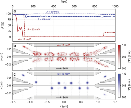
Figure 3. Time-dependent simulation of SAW-driven electron propagation. (a) Qubit fidelity F. (b) Electron wave function Ψ. (c) Trace of Ψ. Reproduced from [158]. CC BY 4.0.
Download figure:
Standard image High-resolution imagede Oliveira Sales et al analyzed the dynamics of a single electron (modeled as a wave packet) in a Morse chain considering SAWs [159]. The considered systems contain two sources of disorder: on-site energies and mass distribution. The authors solve the time-dependent Schrödinger equation.
3.1.4. Levitons
In 1996, Levitov et al advanced the theory of quantum measurement of electric current [160] which together with follow-up work represents the basis for a different type of electron source based on voltage pulses, later named levitons [136]. The fundamental approach is based on applying a periodic train of quantized Lorentzian-shaped pulses to a quantum conductor. Remarkably, this particular pulse shape excites minimal single-electron excitations without generating electron–hole pairs, making leviton single-electron sources an attractive candidate for single-electron sources, in particular for flying qubit systems [6].
Selection of recent computational research: Glattli and Roulleau [161] introduced randomized trains of Lorentzian pulses by using Floquet scattering theory, highlighting the role of the Pauli exclusion principle in electronic quantum signals. These randomized levitons were recently used by Roussel et al to propose a general signal-processing algorithm to extract the elementary single-particle states (the authors refer to these as electronic atoms of signal), see figure 4 [162]. Again, Floquet scattering theory was applied as well as the Wigner function to visualize the single-electron coherence.

Figure 4. Schematic process of extracting single-particle content from a quantum current by using a Hong–Ou–Mandel interferometer, tomographic reconstruction based on the Wigner function, and final calculation of the single-electron coherence via so-called electronic atoms of signal. Reproduced from [162]. CC BY 4.0.
Download figure:
Standard image High-resolution imageYue et al investigated the generation of electron–hole pairs using a scattering matrix approach [163]. Gaussian-shaped voltage pulses and transitions to Lorentzians have been investigated. Among others, it was shown that the electron–hole pairs can always be classified into normal and anomalous electron–hole pairs, whose excitation probabilities depend on the pulse flux.
3.1.5. Locally modulated quantum Hall edge state
In 2018, Misiorny et al theoretically suggested a new type of single-electron source particularly aiming for topological insulators, by applying a local time-dependent gate voltage to create AC pulses in a single quantum Hall edge channel acting as a coherent conductor [137]. A quantum point contact is used as beam splitter. The authors used Floquet scattering theory to analyze different voltage shapes/frequencies and gate geometries.
In follow-up work, Dashti et al used again a Floquet scattering matrix approach to compare the proposed single-electron source approach based on a locally modulated quantum Hall edge state with conventional approaches, i.e., mesoscopic capacitors and levitons [164]. In particular, the authors conducted detailed analyses regarding the temperature dependence of the time-resolved charge and energy currents of the investigated single-electron sources.
3.2. Waveguides and electron dynamics
Generating individual electrons reliably is one thing, another is where to inject them into and how to coherently transfer them via waveguides (a term stemming originally from the field of microwaves and which has later been also introduced to the field of optics). Ultimately, electron sources and waveguides enable one to realize quantum circuits [165] which can be used, for instance, for the previously hinted interference experiments (section 3.3). As discussed, among the most used approaches are quantum Hall edge channels. Historically, such channels have been implemented by using a 2D electron gas (2DEG) in a GaAsAl/GaAs heterojunction which is exposed to a magnetic field so as to realize a quantum Hall regime [166] with no spin degeneracy and long decoherence lengths resulting in a 1D transport channel [15, 167–170]. However, with advances in materials science, alternative materials have been suggested [171].
Selection of recent computational research: Roussely et al conducted time-of-flight measurements of ultrashort few-electron charge pulses injected into a quasi 1D quantum conductor [172]. The density profile in the conductor was calculated using the Schrödinger equation and KWANT [74].
Nedjalkov et al introduced a gauge-invariant Wigner theory in terms of the kinetic momentum which is conserved after a change of the gauge [98]. As a consequence the authors were able to derive an explicit form of the Wigner transport equation corresponding to general, inhomogeneous, and time-dependent electromagnetic conditions.
In follow-up work, Ballicchia et al applied parts of this theoretical framework (by utilizing the Wigner signed-particle formulation provided in the ViennaWD simulator [101, 102]) to investigate the effect of a uniform magnetic field on the electron state interference pattern which arises in a focusing double-well potential structure [173]. The authors analyzed the electron density and the negativity of the Wigner function and showed how the magnetic field controls the electron state but also destroys the coherence of the evolution dynamics.
In related work, Ballicchia et al presented an analysis of the quantum processes involved in the electron evolution around a barrier placed in a waveguide using ViennaWD [174]. The quantum transport results have been compared to classical results (an inherent ability of a Wigner transport approach) to better highlight quantum effects. The relation between quantum effects and their impact on the current has been highlighted. In follow-up work, the authors introduced an approach for modeling surface roughness in waveguides [175] and investigated the relation between quantum coherence, interference, and the negative parts of the Wigner quasi-distribution in a beam splitter structure using ViennaWD [176].
Weinbub et al investigated single-electron interference effects as a result of interactions between single-electrons and two potential wells symmetrically placed in a waveguide, again using ViennaWD [177]. The results bear resemblance to the well-known double-slit experiment. The tight dependence between the well configurations (e.g., size, position) and resulting interference pattern triggered follow-up research with respect to a potential application as logic devices [178], see figure 5.
Figure 5. 2D quantum electron density (a.u.) as computed by a Wigner signed-particle approach for a bottom-injected, single-electron device. Two gate-driven quantum wells (green: positive bias, yellow: negative bias) control the interference pattern and thus the current in the three top output channels separated by rectangular potential barriers (white). Reproduced from [178]. CC BY 4.0.
Download figure:
Standard image High-resolution imageRodriguez et al used a scattering matrix approach to investigate experimental findings concerning the relaxation and revival of electrons injected at finite energy into a quantum Hall edge channel [179].
Sanz et al theoretically investigated the use of two crossed graphene nanoribbons for use as a beam splitter or mirror [180]. The authors used tight-binding, DFT, and Green's function theory to calculate the electron transport properties.
Ito et al developed a coherent beam splitter for single electrons driven through two tunnel-coupled waveguides by SAWs [181]. The authors solved the Schrödinger equation to describe the SAW-driven electron transport. A relation between the gate voltages and the current oscillations in the wires is being shown and related to the coherent electron tunneling.
Moreau et al investigated limitations of realizing quantum Hall edge channels in graphene [182]. The authors particularly looked at the combined role of electrostatics and antidots at graphene edges in quantum Hall breakdown. Tight-binding simulations provided by KWANT [75] were used to tune the position and configuration of the quantum Hall edge channels by optimizing the utilized scanning gate microscopy's tip voltage and position (figure 6).
Figure 6. Tip-controlled tuning of transport through a quantum Hall edge channel island in graphene. (d) Simulation setup and potential landscape. The antidot is represented by a circular region with low potential, 45 nm from the graphene edge. Four contacts are used (yellow). (e) Profile of the three lowest Landau levels along the black dashed line in (d). (f)–(h) Simulated current density maps for different tip positions. Reproduced from [182]. CC BY 4.0.
Download figure:
Standard image High-resolution imageVarnava et al evaluated quantum point junctions on the surface of an antiferromagnetic topological insulator [171]. Antiferromagnetic topological insulators have been predicted by Mong, Essin, and Moore in 2010 [183]. Since then several material candidates have been identified, such as MnBi2Te4, MnBi4Te7, EuIn2As2, and NpBi, promising high temperature operation (contrary to conventional 2DEG systems). It this recent work, the authors used dynamic wave-packet simulations to extract the scattering-matrix of the quantum point junction.
Rebora et al studied electron–electron interactions between two edge channels at filling factor two considering electromagnetic radiation generated by a quantum Hall device in a quantum point contact geometry [184]. The two interacting quantum Hall edge channels are modelled using the edge-magnetoplasmon scattering matrix formalism.
Welland and Ferry developed a novel numerical method for solving the Wigner transport equation, without relying on evaluating the Wigner kernel [185]. The authors evaluated their method by simulating and analyzing a cat state, entangled Gaussians, and excited states.
In follow-up work to [186], Jensen et al developed a novel numerical solution to the time evolution equation of the Wigner distribution function [187]. A particular focus was to correctly capture the intricate dynamics of an impinging wave packet (electron) on a barrier (focus on Gaussian and parabolic), exhibiting transmission and reflection behavior, i.e., transmission and reflection delay times. The newly developed solution approach relies on the finite difference method using second-order accurate schemes in both position and momentum.
Benam et al introduced a computational approach for investigating Coulomb interaction using Wigner–Poisson coupling, thereby providing an option to investigate dynamic electron–electron entanglement [188]. The authors apply an approximation based on replacing the Wigner potential of the electron–electron interaction by a local electrostatic field, which is introduced through the spectral decomposition of the potential.
3.3. Interferometers
Based on research into electron sources and additional work on ballistic conductors, it became possible to investigate the fundamental wave-based quantum properties of electrons by conducting experiments similar to the quantum optical domain, most dominantly, interference experiments, such as Fabry–Pérot [16], Mach–Zehnder [17], Hanbury Brown–Twiss [18], and Hong–Ou–Mandel [19] interferometers. The reader is directed to the review of Bäuerle et al concerning an overview of various electron-based interferometers [6].
Selection of recent computational research: Barbarino et al considered a Hong–Ou–Mandel interferometer and showed how to engineer statistical transmutation of identical quantum particles, in particular, to cause fermions to bunch [189]. To that end, the authors used a scattering matrix approach and suggested to entangle the quantum particles with an external degree of freedom.
Bordone et al reviewed an approach where the Schrödinger equation is solved with a split-step Fourier method for interferometers based on quantum Hall edge channels [190]. Using this modeling and simulation framework, in earlier work, Bellentani et al investigated a multichannel electronic Mach–Zehnder interferometer, based on magnetically driven noninteracting edge states [191]. Later, the antibunching of two interacting fermionic wave packets impinging on a quantum point contact considering a Hong–Ou–Mandel interferometer based on quantum Hall edge states was simulated [192]. In follow-up work, single and two-electron transport in a full-scale, 2D Hall nanodevice as a potential candidate for a two-qubit conditional phase shifter was investigated [193]. The authors considered two parallel Mach–Zehnder interferometers, see figure 7. In particular, the spatial shift induced by Coulomb repulsion in the final two-electron wave function for two indistinguishable electrons was shown and discussed.

Figure 7. Design of a conditional phase shifter based on two Mach–Zehnder interferometers. Reprinted (figure) with permission from [193], Copyright (2020) by the American Physical Society.
Download figure:
Standard image High-resolution imageAcciai et al studied the interplay between electron excitations, considering levitons, and electron–electron interaction in an integer quantum Hall system [194]. The authors showed that the excitations fractionalize into oppositely charged wave packets and show the derivations of the used equations of motion as well as using the Wigner function for visualizing the excitations.
Clark et al studied the decoherence mechanisms of hot electrons in a Mach–Zehnder interferometer, particularly focusing on acoustic and optical phonon emissions [170]. The authors used a quantum master equation for the electron density matrix based on rates derived from the Fröhlich Hamiltonian modified to include emission within interferometer arms.
Rebora et al investigated a Hong–Ou–Mandel interferometer with levitons injected into a quantum Hall edge channel [195]. A particular focus was on the relation between noise and the geometry of the setup. The dynamics of the two interacting quantum Hall edge channels are modelled in terms of the edge-magnetoplasmon scattering matrix formalism.
Kotilahti et al investigated multi-particle effects in an electronic Mach–Zehnder interferometer driven by a series of voltage pulses [196]. The authors used the Floquet scattering formalism to evaluate the interference current and the visibility in the outputs of the interferometer.
3.4. Tomography, spectroscopy, and detection
With the ability to reliably generate and transport single-electrons the natural next step is to be able to characterize them. This gives rise to tomography, spectroscopy, and detection techniques. This section summarizes a few key computational research advances in this setting.
Selection of recent computational research: in general, quantum tomography refers to extracting and analyzing the wave function of single-electron excitations [197]. In 2019, Bisognin et al introduced a quantum tomography protocol for generating electron and hole wave functions and their emission probabilities from any electrical current, focusing in particular on levitons [198], see figure 8. The authors evaluated the electron/hole wave functions based on calculated Wigner distributions using Floquet scattering theory.

Figure 8. Electron wave function generated by a Lorentzian pulse and described by Wigner function reconstruction. Reproduced from [198]. CC BY 4.0.
Download figure:
Standard image High-resolution imageFletcher et al introduced a continuous-variable, back-projection-based tomography scheme of solitary electrons [199]. The authors used energy-time filtering and reconstruction of the mixed-state density matrix Wigner representation.
Locane et al investigated single-electron scattering by a ballistic constriction in a fully depleted quantum Hall system under spatially uniform but time-dependent electrostatic potential modulation [200]. The authors applied the Wigner function to describe electrons distributed in time-energy space.
In contrast, spectroscopy provides insights into the time-frequency dependencies of the quantum systems. In 2018 Rossignol et al proposed a spectroscopy approach of flying qubits, by measuring the direct-current (DC) response to a high-frequency AC voltage drive [201]. The authors used Floquet theory and conducted time-dependent simulations based on different models and predicted the power-frequency map of the multi-terminal device using KWANT [74].
Burset et al proposed time-domain spectroscopy of waveguides by applying Lorentzian-shaped voltage pulses (levitons) to an input contact [165]. Floquet scattering theory was used to calculate the electron waiting times, considering an electronic Fabry–Pérot cavity and a Mach–Zehnder interferometer. The authors showed how the distribution of waiting times between charge pulses relates to the characteristic timescales of the waveguide.
In turn, Zilberber et al studied electron detection considering coherent transfer via adiabatic passage in a triple quantum-dot system, where a quantum point contact senses the charge of the middle dot [126]. The authors apply a Bayesian formalism based simulation to study the measurement backaction.
4. Quantum dots and spin qubits
As previously indicated, different approaches for realizing a competitive quantum information processing platform are being investigated. Contrary to section 3, here we focus on one of the primary platforms to realize such a system, spin qubits based on quantum dots, which is based on the original proposal by Loss and DiVincenzo in 1998 [202]. These quantum dots are typically implemented by impurities or gate-defined potential wells and the qubit is realized via spin orientations influenced by a magnetic field. For excellent in-depth reviews (also concerning alternative approaches, e.g., superconducting systems) see [9, 203–208]. In what follows we highlight several contributions in the context of quantum dots and spin qubits where computational methods played a key role in the presented results.
Selection of recent computational research: Watson et al demonstrated a programmable two-qubit quantum processor in a silicon device and showed the operation based on the Deutsch–Josza and Grover search algorithm [209]. The authors conducted numerical simulations where they considered two electrons in two tunnel-coupled quantum dots with an external magnetic field applied to both dots. They solved the dynamics of this system with the Schrödinger–von Neumann equation.
Mohiyaddin et al introduced a multiphysics simulation approach for designing silicon qubit devices [210]. By way of example, a Si-MOS, gate-defined two-qubit device is used as an evaluation platform. The electrostatics of the dots are numerically investigated by self-consistently solving the Schrödinger–Poisson equations.
Lepage et al described an approach to entangle spin qubits within moving quantum dots (i.e., SAWs) [211]. The authors used graphics processing units to simulate the wave function dynamics of two electrons carried by a SAW through a 2D semiconductor heterostructure. The authors solve the time-dependent Schrödinger equation using a staggered-leapfrog method.
Yazdani et al studied carrier transport, generation, and trapping in nanocrystal quantum dot-based semiconductors using DFT [212]. The authors used CP2K [68] to calculate the electronic structure.
Niquet et al discussed the challenges and perspectives in modeling spin qubits [213]. In particular, the authors make the case for establishing quantum computer-aided design as the key required simulation-based toolchain which will enable the success of solid-state based quantum information processing platforms. To that end, the authors identified structural, electro-magnetic, electronic structure (k ⋅ p, tight-binding), electron interaction (Schrödinger–Poisson or better), and qubit dynamic and operation (time-dependent Schrödinger or better) modeling and simulation as the key elements of the envisioned toolchain.
In similar work, Asai et al introduced a device simulator specifically tailored to qubits [214] using in-house tools [215]. The authors envision the following toolchain: (i) self-consistent quantum simulation of the quantum dot (Schrödinger–Poisson) coupled with semi-classical modeling (drift–diffusion-Poisson) for device interfaces; (ii) quantum dot capacitance calculation; (iii) micromagnetic simulations; (iv) single-electron quantum transport via Schrödinger equation (with magnetic field).
Pont et al studied inter-Coulombic electron capture in nanowire-embedded quantum-dot pairs, considering electron emission in one quantum dot triggered by electron capture in the other dot [216]. The authors used a multi-configuration time-dependent Hartree approach [217, 218] to calculate the electron dynamics in general binding potentials.
Santos et al theoretically investigated the transmission of a two-electron quantum state between the leads of a chaotic quantum dot [219]. The chaotic nature of the system required a statistical approach to describe the electron dynamics. To that end, the authors used the scattering matrix formalism in combination with Wigner–Dyson circular ensembles of random matrices to study the fidelity of orbital state transfer in the quantum dot.
Bush et al depicted a master equation approach to simulating transport through quantum dots targeted for educational purposes [220].
Hu et al introduced a machine learning approach for solving the quantum conditional master equation for qubits [221]. More concretely, the authors used a long short-term memory network [222] to study the two-level quantum qubit transport problem.
Bogan et al (contrary to the approaches discussed so far) focused on hole spins as qubits and analyzed the magneto-transport of a gated lateral GaAs double quantum dot [223]. The authors applied the density matrix formalism to simulate the tunneling current, see figure 9.

Figure 9. Comparison of the measured (left) and simulated (right) tunneling current in a two-hole double quantum dot setup as a function of the gate voltage and the magnetic field. Reprinted (figure) with permission from [223], Copyright (2021) by the American Physical Society.
Download figure:
Standard image High-resolution imageGinzel et al theoretically investigated spin shuttling between semiconductor quantum dots [224]. Spin shuttling refers to a bucket-brigade transport style between neighboring empty quantum dots [225]. The electron dynamics during a detuning sweep in a silicon double quantum dot occupied by one electron was analyzed. The authors calculated the spin shuttling infidelity by numerically integrating the time-dependent Schrödinger equation with degenerate spin levels during a finite-time detuning sweep.
Buonacorsi et al introduced a design for a large-scale surface code quantum processor based on a node/network approach and on spin qubits [226]. The approach relies on electron shuttling to distribute entanglement between adjacent nodes. The authors used a three-dimensional (3D) Poisson solver to calculate the potential landscape. Individual 1D slices of the potential profile were used for the shuttling simulation based on solving the time-dependent Schrödinger equation. In follow-up work, the work was extended towards more realistic device scenarios by optimizing the shuttling voltage sequences and the device geometry [227]. The shuttling of single electrons in gate-defined silicon quantum dots was simulated using the split-operator approach for solving the time-dependent Schrödinger equation.
5. Superconducting junctions
Among the focus areas of research into superconducting systems are interfaces between metals and superconductors. Considering current flow, at such an interface Andreev reflection [228] (also referred to as Andreev processes) manifests itself, i.e., the conversion of electrons in the metal to Cooper pairs in the superconductor. Andreev reflection is the essential mechanism for the supercurrent flow in Josephson junctions. Of course, yet another important and related research area are superconducting qubits; for a recent review see [207].
Selection of recent computational research: Mi et al investigated the waiting time distributions of superconducting hybrid junctions based on conventional and topologically nontrivial superconductors [229]. The authors employ a scattering matrix formalism for evaluating the waiting times between the transmissions and reflections of electrons or holes. It was demonstrated that the waiting time distributions of Andreev processes are sensitive to topological edge states.
Rossignol et al introduced a computational framework for microscopically describing Josephson junctions considering an attached electrical circuit [230]. In essence, the resistor capacitor Josephson model is merged with the Bogoliubov–De Gennes equation, providing a self-consistent treatment of the Josephson junction and its electromagnetic environment. Among others, this approach allows to describe non-equilibrium phenomena such as multiple Andreev reflection. The system of equations is solved within the Keldysh formalism, ultimately requiring to solve a plethora of time-dependent Schrödinger equations, for which the authors used an at that time unreleased version of TKWANT, which has been released in the meantime [75].
Nowak et al theoretically studied coherent multiple Andreev reflections in a biased three-terminal Josephson junction [231]. The authors used a scattering matrix approach to calculate and analyze the current through the junction and compared the results with conventional experiments, see figure 10. In related work, Belogolovskii et al used scattering theory to investigate transport across a three-arm beam splitter made by different superconducting wires [232].

Figure 10. Calculated DC (top) and differential conductance (bottom) in one of the leads of a Josephson junction. Reprinted (figure) with permission from [231], Copyright (2019) by the American Physical Society.
Download figure:
Standard image High-resolution imageDamanet et al introduced an approach to study dissipative control of transport in strongly interacting fermionic systems considering a superconducting lead-quantum dot-superconducting lead tunnel junction [233]. Among others, the relation between superconducting leads and subgap currents exhibiting multiple Andreev reflections was discussed. The authors derived a Floquet–Born–Markov master equation which allows to describe multiple Andreev reflections.
Averin et al extended the theory of Andreev reflection in a normal metal-superconductor junction to include an arbitrary time-dependent bias voltage across the junction [234]. The authors solve the Schrödinger equation to describe the wave function of an electron crossing the metal–superconductor junction.
Another intriguing superconducting system is a superconducting quantum point contact [235]. Here, two superconducting electrodes are connected by a narrow constriction, where the length of said constriction is much smaller than the superconducting coherence length. Acciai et al investigated the transport properties of a superconducting quantum point contact (in the tunnel regime) considering an arbitrary periodic drive (Levitons) [236]. In particular, the authors extended the research into Coulomb interaction based electronic correlations (as done with the field of electron quantum optics) to the superconducting domain. The authors used an NEGF approach to calculate the direct current across the junction and the zero-frequency noise at lowest order in the tunneling amplitude.
6. Material systems
The success of electronic systems is inherently linked to advances in materials science. For instance, the understanding of silicon and its oxide was vital for the development and astounding success of microelectronics and remains a key driver until today. Another example are semiconductor light-emitting diodes, which of course rely on direct semiconductors, such as InAs and GaAs. Materials science in general has benefited from computational tools since a long time [10, 63–65, 67, 68, 237–241]. In particular, first-principles methods, such as DFT, have been key enablers to advance the understanding of known materials and also predict entirely new materials.
6.1. 2D materials
As previously indicated, the high pace of research in electronic devices has been fueling massive research efforts into novel materials. With the advent of graphene in 2007, 2D materials entered the race and have since then evolved into a major field of research giving rise to a plethora of new very exciting electronic materials, e.g., MoS2 and many others [8]. In the following we list several advancements in computational materials science where treating electron transport quantum mechanically is vital for the gathered findings. We first start with graphene followed by research into other 2D materials.
Selection of recent computational research: Mosallanejad et al investigated the electronic transport properties of curved graphene waveguides by using an NEGF approach [242]. In particular, the authors studied the dependence of the confined waveguide modes on the potential difference, waveguide width, and side barriers. In similar research, Wei et al used graphene waveguides to build and analyze a four-terminal gate defined waveguide and an Aharanov–Bohm interferometer [243]. The authors used an NEGF approach (Landauer–Büttiker for spin-dependent current) and highlighted and discussed the predicted conductance plateaus and relations to experimental results.
Espinosa-Torres et al used DFT, molecular dynamics, and NEGF to theoretically analyze the electronic structure and transport properties of several single and double walled carbon nanotube configurations to identify optimal configurations [244].
Santos et al used a graphene Hall bar to introduce a novel self-contained description of the wave-function matching method to calculate electronic quantum transport properties of nanostructures using the Landauer–Büttiker approach [245]. The method is based on partitioning the system-to-be-solved into a central conductor and an asymptotic region for the leads. The thus resulting two subsystems are linearly coupled and can be solved simultaneously using a sparse linear solver.
Yamaletdinov et al used stochastic reactive molecular dynamics simulations for developing a statistical method for generating fluorinated graphene structures with a desirable fluorine distribution [246]. In addition to molecular dynamics, the transport properties are investigated using a recursive NEGF method based on a tight-binding Hamiltonian.
Díaz-Bautista et al used the Wigner function for analyzing the electron dynamics of uniaxially strained graphene [247]. In particular, the authors studied the effect of strain on the Wigner function of electrons considering a uniform magnetic field, see figure 11. It was shown that strain impacts the shape of the Wigner function of Landau and coherent states.
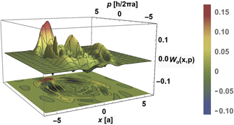
Figure 11. Snapshot of the trace of the calculated Wigner matrix describing electron dynamics in strained graphene. Reprinted (figure) with permission from [247], Copyright (2020) by the American Physical Society.
Download figure:
Standard image High-resolution imageKraft et al investigated graphene superlattice miniband fermions using interferometry in magnetotransport experiments and tight-binding and Green's function quantum transport simulations [248]. The results revealed unconventional cyclotron motion on the length scale of the cavity, which reflects the reshaped hexagonal Fermi surface.
Silva et al used time-dependent DFT to investigate negative differential conductance, current oscillations, and molecular sensing in isolated finite armchair single wall carbon nanotubes without end contacts [249]. The authors showed that (i) the conductivity depends on the nanotube length, (ii) the nanotube current has Bloch oscillations, and (iii) that the adsorbed molecule on the nanotube impacts this oscillatory pattern, decreasing the conductivity.
Solomon et al analyzed valleytronic phenomena in graphene using a Schrödinger equation approach [250]. In particular, it was shown that strong valley-dependent scattering emerges from bilayer graphene quantum dots. Dots of course allow for tuning as the gap size can be modulated using the interlayer potentials in dual-gated devices. The authors investigated the role of dot size, mass strength, and other potential terms.
Barletti et al derived a mathematical model describing a general graphene heterojunction device consisting of two classical regions (diffusive transport) and one middle active region (quantum transport) [251]. Where the first are modelled by a conventional drift–diffusion modeling approach, the latter is modelled by an interface where suitable transmission conditions are imposed, which take the quantum scattering process into account.
Aktor et al used a combination of quantum transport formalisms (Green's function, Kubo, and Landauer–Büttiker formalisms) to discuss bulk and valley-polarized currents in graphene-based devices which are driven by spatially varying regions of broken sublattice symmetry [252]. The findings represent alternatives for generating the valley Hall effect in graphene and for valley-dependent electron optics.
We now turn to other 2D materials beyond graphene. As indicated before, there is a plethora of predicted and investigated 2D materials providing various advantages but also disadvantages. Klinkert et al conducted a large-scale computational study to investigate the suitability of 100 different 2D materials for potential use in ultra-scaled FETs [8]. To that end, the authors applied DFT and quantum transport simulations using OMEN (Schrödinger–Poisson solver via an NEGF formalism) [253] to calculate current–voltage characteristics for each material. In another review, Wang et al provided an overview on the advancements concerning Schottky barriers within the context of FETs based on 2D materials [254]. The authors investigate both theoretical and experimental work and identify in particular first-principles simulations to be most crucial for advancing the research in this area.
Ferry et al investigated the use of the Wigner function for describing transport in transition metal dichacogenides (WS2) with a dominant spin–orbit interaction [255].
Szafran et al studied electron transport, in particular electron wave packet dynamics, along the zero line of a symmetry-breaking potential of a vertical electric field in buckled silicene [256], see figure 12. The authors used an atomistic tight-binding approach and solved the Schrödinger equation on the atomic lattice; for the initial conditions an analytical solution of the Dirac equation was utilized.

Figure 12. Time evolution of the wave packet without (top row) and with (bottom row) applied magnetic field. Reproduced from [256]. CC BY 4.0.
Download figure:
Standard image High-resolution imageQu et al studied the electronic properties of 2D Sb2Te2Se and its use in a double-gated MOSFET by coupled DFT–NEGF simulations [257]. Monolayer Sb2Te2Se offers some intriguing properties, such as high carrier mobility, and the authors show that in particular the n-MOSFET is attractive because of a much higher on-current.
Zhang et al introduced an implementation of the exact muffin tin orbital method in combination with Kohn–Sham DFT for electronic-structure and quantum transport simulations [258]. The authors considered a representative device-material system in equilibrium condition based on, e.g., MoS2 and black phosphorus, as evaluation platform and used the recursive Green's function method to calculate the device region.
Hu et al used DFT coupled to NEGF to investigate the electronic properties and ballistic transport performance of 2D SbSiTe3 [259]. This particular material has attractive properties and a layered structure, thus monolayers can be created via exfoliation. The authors used a double-gated MOSFET device structure as benchmark platform.
6.2. Topological materials and systems
Topological materials have an electronic band structure that has a band topology and offer topologically protected surface states with unique electronic properties (for a recent review on topological nanomaterials see [260]). Research into topological materials focuses, among others, on 2D materials, topological (crystalline) insulators, topological semimetals, topological superconductors, fractional quantum Hall effect, quantum rings, and Majorana zeromodes [260, 261].
Selection of recent computational research: Gioia et al used a scattering-matrix approach to calculate the electronic two-terminal conductance (including interference effects) of a quantum ring, considering Dirac-like charge carriers as are typical for 2D materials [262]. The authors apply a k ⋅ p approach to describe the Dirac-electron rings.
Rodríguez-Mena et al investigated the transport of the anomalous Floquet-Anderson insulator which is a topological phase unique to driven systems [263]. The authors used Floquet scattering theory for the transport calculations.
Wu et al used an NEGF approach to study the transport properties of the edge modes of a Fe3Sn Kagome nanoribbon [264]. Kagome lattice materials are layered 2D materials and can possess topologically non-trivial electronic bands and are an attractive candidate as an interconnect material.
Ronetti et al analyzed the transport properties of a single edge of a 2D topological insulator (with Rashba spin–orbit coupling) which is driven by a train of Lorentzian-shaped pulses (levitons) and connected to a superconductor [265]. The suggested setup represents an alternative realization of an electron quantum optics experiment where the beam splitter is realized by the superconductor rather than a quantum point contact. The authors calculated the charge noise and derived the equations of motion for their setup and used the scattering matrix approach to take the effect of the superconductor into account.
Okugawa et al studied disorder induced topological phase transitions in magnetically doped (Bi, Sb)2Te3 thin films [266]. To that end, the authors used Landauer–Büttiker theory to calculate the disorder averaged conductance and compare their exact disorder simulation results with a self-consistent Born approximation.
Huang et al derived the exact master equation and transient quantum transport for studying dissipative topological systems, focusing on non-interacting topological insulators and topological superconductors and including initial system-reservoir entanglement [261]. The authors show that the dissipative dynamics is fully encapsulated in the spectral density through NEGFs.
Cepellotti et al introduced a first-principles model for electronic transport using the Wigner distribution function and used it to solve the electrons' equations of motion in Bi2Se3 [267], see figure 13. It was shown that interband tunneling dominates the electron transport dynamics.

Figure 13. 2D histogram of calculated contributions to electrical conductivity as a function of two interacting carriers: the authors identified on-diagonal elements as ab initio Boltzmann transport equation like terms and the important off-diagonal elements provided by ab initio Wigner transport. Reproduced from [267]. CC BY 4.0.
Download figure:
Standard image High-resolution image6.3. Light–matter interaction
Light–matter interactions are quantum electrodynamical processes and typically described by electron quantum transitions and cover emission, absorption, and scattering of electromagnetic field quanta [268]. Here, we introduce computational research covering solar cells, photovoltaic effect, and LASER based energy transfer.
Selection of recent computational research: Hathwar et al published a review on the role of ultrafast carrier dynamics in the performance of advanced concept solar cells [269]. Aside from theoretical work, the authors particularly highlighted computational results based on ensemble Monte Carlo transport simulations and focused on multi-quantum well systems and as well as III–V nanowires. Li et al reviewed research focusing on excited state dynamics in perovskite solar cells [270]. Many other reviews on this topic exist, see for example an extensive review by Moskalenko et al [271].
Michelini et al introduced a theoretical framework to describe time-dependent energy transport in quantum networks, in particular focusing on energy transfer from a femtosecond LASER pulse to electrons and subsequent transport in a molecular circuit [272]. The authors used an NEGF approach to simulate the energy current in the system.
Bajpai et al conducted a computational study of shift current (a central mechanism of the bulk photovoltaic effect) dynamics in response to a femtosecond light pulse [273]. To that end, the authors employed a time-dependent NEGF approach to simulate the current dynamics.
Beltako et al used an NEGF approach to calculate the charge transfer dynamics triggered by a femtosecond LASER pulse at the donor–acceptor interface of molecular junctions [274] (for molecular junctions, see also section 6.5). The authors include Coulombic interaction within the Hartree–Fock approximation.
Aeberhard conducted a computational study of hot carrier photocurrent generation in quantum well solar cells using an NEGF approach [275, 276]. The author included GW self-energy to treat electron–electron scattering together with photogeneration and phonon-mediated carrier relaxation.
Karlsson et al introduced an NEGF approach for describing electron-boson dynamics with a particular focus on computational efficiency (numerical effort scales linearly with propagation time) and upholding the conservation law [277]. Figure 14 depicts the simulated electron–phonon dynamics in the considered showcase system.

Figure 14. Electron–phonon dynamics triggered by a laser pulse in a narrow band-gap insulator consisting of one valence and one conduction band. Insets depict respective populations at the end of the evolution. Reprinted (figure) with permission from [277], Copyright (2021) by the American Physical Society.
Download figure:
Standard image High-resolution imageTang et al investigated the layer-dependent photoresponse properties and photovoltaic effects of 2D Bi2O2X (X = S, Se, and Te) by combining first-principles calculations and quantum transport [278]. In particular, the authors calculated the absorption coefficients via time-dependent DFT and the photocurrent via an NEGF method.
6.4. Heterostructures and interfaces
Heterostructures consist of several combined materials with the typical motivation to improve the intrinsic characteristics of an individual material. Heterostructures are a success story and there are countless examples, both historically and in modern times, in particular with the advent of 2D materials. Practically, all modern electronic devices are actually heterostructures so it is hard to draw a clear line here. However, here in this section, we present computational research where the focus is on the heterostructure itself rather than on a complete device. For a recent overview on this matter see [279].
Selection of recent computational research: Jech et al used ab initio methods to study the interactions of a Si–H bond in a 3D Si/a-SiO2 interface [280]. In particular, the authors used well-tempered metadynamics and nudged-elastic-band calculations based on DFT (via the CP2K package [68]), which allowed them to shed light on the dissociation kinetics and electronic properties.
Dong et al introduced atomistic full-band self-consistent quantum transport simulations of the graphene/MoS2 edge contact using a Wannier-function basis [281]. The authors used DFT to obtain the band structures and for the quantum transport solver they applied the NEGF formalism and maximally localized Wannier functions.
Xu et al presented a computational study about the ohmic contact at bilayer InSe–metal interfaces within the context of FETs [282]. The authors employ DFT and ab initio quantum transport simulations [52]; the latter is particularly useful for correctly describing the lateral Schottky barrier heights.
Szabó et al used ab initio quantum transport simulations to investigate the role of an oxide layer between a metallic contact and a MoS2 monolayer [283]. The authors analyzed the interface related edge- or area-dependent electron transport processes. The computational methodology consisted of combining plane-wave DFT, maximally localized Wannier functions, and NEGF.
Yang et al looked at ballistic transport properties with a particular focus on a change of the Hamiltonian in a lead-semiconductor-lead structure (1D atom chain model) [284]. A NEGF approach was used to derive the transient current.
Ning et al used ab initio electronic calculations and quantum transport simulations to investigate the electronic and transport properties of InAs/graphene heterostructures [285]. More specifically, the authors used VASP [65] for the DFT part and interfaced it with NEGF based transport simulations [52].
Bhattacharya et al investigated the bridge-site asymmetry for methanethiol adsorbed on Au(111) with two different S–C bond orientations using dispersion-corrected DFT [286]. Again, VASP [65] was used and various configurations regarding pseudo-potentials, exchange functionals, and dispersion correction were considered for optimal modeling.
Ducry et al introduced a mode-space approximation for transforming the Hamiltonian of a metallic structure expressed in a nonorthogonal DFT basis into a low-dimensional space suitable for electron-transport simulations, in particular for NEGF [287]. The authors applied it locally to inhomogeneous material stacks including amorphous phases and interfaces. Figure 15 shows simulation results for a Cu/a-SiO2/Cu conductive bridging random-access memory cell structure.
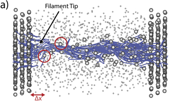
Figure 15. Simulated current field lines for the considered atomistic representation of a Cu/a-SiO2/Cu conductive bridging random-access memory cell structure under an applied bias. Reprinted (figure) with permission from [287], Copyright (2020) by the American Physical Society.
Download figure:
Standard image High-resolution imageM'foukh et al discussed a full-band quantum transport model based on the NEGF formalism and empirical pseudopotentials and the application to heterojunctions between lattice-matched semiconductors [288]. The authors also applied their method to an Esaki tunneling diode and n- and p-type heterojunction tunnel FETs.
Smorka et al investigated non-equilibrium steady-state charge transport through a heterostructure consisting of a finite 2D lattice (Falicov–Kimball model) which is sandwiched between two non-interacting semi-infinite leads [289]. A particular focus was on the influence of non-homogeneous charge orderings on the transport. The computational approach was based on a Monte Carlo-NEGF solver.
Kumar et al studied the low field 2DEG transport properties in  heterostructures [290]. The authors used a self-consistent Poisson–Schrödinger solver to calculate the sub-band energies and the wave functions in the quantum well. In turn, DFT (and density functional perturbation theory) was used to determine the phonon dispersion.
Li et al used neural networks to predict transport properties of a quasi-1D tight-binding model with disordered on-site energies [128]. The authors consider a scattering region between two leads as the evaluation platform. Different disorders of the on-site energies in the scattering region are considered.
Wu et al introduced a machine learning approach to replace NEGF quantum transport simulations and used as a showcase a simulation of a graphene–ferroelectric–metal ferroelectric tunnel junction [291]. Their approach is based on learning a sparse representation of a quantum transport property, which allows to train a model to yield device properties.
Wang et al investigated van der Waals p–n heterojunctions considering 2D–2D (e.g., black phosphorus/MoS2) and mixed dimensional systems [292]. The interface physics is investigated by means of quantum transport simulations (encompassing incoherent scattering and carrier recombination). The transport simulations were based on an NEGF method (NEMO5 [50]) in combination with maximally localized Wannier function basis sets created for structures relaxed within DFT models (VASP [65]).
Jin et al used a Schrödinger–Poisson approach to calculate the dynamical electron transmission in an ultra-short two-terminal piezoelectronic device (ballistic regime) [293]. A metal–piezoelectric ZnO–metal structure exposed to sinusoidal and rectangular external stresses was considered.
6.5. Molecular junctions and systems
This section discusses computational research into the electronic characteristics and electron transport in molecular junctions and systems. The majority of research focuses on junctions, where a metal–molecule–metal configuration is considered. However, other molecular systems are considered as well, such as loop structures. Excellent recent reviews on computational methods for molecular junctions cover electron transport [294] and specifically the use of Green's function methods [295].
Selection of recent computational research: Avriller et al investigated time-dependent electronic transport properties and vibrational dynamics of a molecular junction based on an NEGF approach [296]. Among others, the authors identify oscillations and establish a similarity with the classical harmonic oscillator.
Moura-Moreira et al analyzed electron tunneling through two 1D molecular junctions using a coupled DFT and NEGF approach [297]. The first junction consists of left and right carbyne wire electrodes with a sodium atom in the middle. In contrast, the second junction is based on two single-wall carbon nanotube electrodes with again a sodium atom in the middle, the scattering region.
Pohl et al presented time-dependent electron transport simulations through a graphene nanojunction under time-dependent potential biases [298]. The authors used the driven Liouville–von Neumann approach to simulate the one-electron density matrix dynamics under non-equilibrium conditions and to analyze scattering and relaxation processes as well as the steady-state, see figure 16.
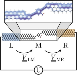
Figure 16. The oligo-(phenylene-ethynylene)-graphene nanoribbon model system is shown including an overlay of the simulated electronic current density as a streamline plot for a representative snapshot. Reprinted with permission from [298]. Copyright (2019) American Chemical Society.
Download figure:
Standard image High-resolution imageChiang et al discussed time-dependent electron transport simulation results of a molecular junction (fumaronitrile molecule) in the adiabatic limit using DFT and the molecular dynamics-driven Liouville von Neumann (MD-DLvN) approach [299]. The modeling was done within the Born–Oppenheimer approximation, i.e., no vibronic coupling, and ignoring nuclear quantum effects.
Phuc et al showed that the electron transfer dynamics in molecular loop structures can be manipulated by Floquet engineering (i.e., Hamiltonian of the system is temporally modulated in a periodic manner) via LASER pulses [300].
Liu et al introduced the generalized input–output method for studying charge transport in molecular junctions considering strong electron-vibration interactions and including electronic and phononic environments [301]. The authors derive a Langevin-type equation of motion for system operators and position their framework relative to NEGF and perturbative quantum master equation methods. In follow-up work, the method is applied to various molecular junctions [302].
Ramakrishnan et al studied transport selectivity across isomeric molecular junctions by conducting computational electron dynamics studies considering many-body coherence and electron correlation effects [303]. To that end, the authors employed the real-time, many-body, and time-dependent configuration interaction method to model and simulate the ultrafast electron dynamics [304] and compared the method to Green's function and density matrix approaches. Cyanobenzene and in m/p-linked benzonitrile thiolate molecules bonded to a gold atom (acceptor terminal) were considered. Interference effects in the electron density were observed and discussed.
Tharammal et al discussed a simulation based design for a molecular switch considering a 1.4-benzene dithiol molecule with gold, silver, platinum, and palladium metal electrodes [305]. The electronic properties have been calculated using DFT and the Hartree–Fock method.
Romero-Muñiz et al presented a theoretical study within the context of protein electronics [306]. More specifically, the authors investigated the coherent electron transport in metal–protein–metal junctions based on the blue-copper azurin from Pseudomonas aeruginosa. The simulation methodology was based on molecular dynamics (junction geometries), DFT (electronic structure), and Landauer formalism/NEGF (electron transport).
Tuovinen et al introduced a generalized Kadanoff–Baym ansatz scheme (on top of NEGF theory) which considers initial correlations in a partition-free setting [307]. The method was evaluated considering carbon-based molecular junctions based upon electron correlations in transient current signatures.
Arasu et al employed atomistic simulations to establish a general relationship between the electronic spectra of aromatic, antiaromatic, and quinoidal molecules and the impact on electron transport [308]. To that end, the authors utilized a DFT–NEGF approach for simulating and analyzing the electronic properties.
Cheng et al investigated non-equilibrium transport in conjugated polymer by a time-dependent NEGF approach [309]. Specifically, a polymer chain, using a Su–Schrieffer–Heeger model Hamiltonian, was sandwiched between two reservoirs.
7. Field-effect transistors
Lilienfeld's patent for a transistor has been granted over 90 years ago [310] and, most astoundingly, to this day the transistor is the core device of the electronics industry and will remain so for the foreseeable future. Of course, device designs and material systems have advanced over time and in particular the feature sizes have decreased; both will continue to do so even if approaching atomistic limits requires alternative device designs. Over large parts of the transistor's history, the fundamental electrical characteristics could be modelled in a classical manner: the introduction of the effective mass enabled this simplification, allowing to hide quantum mechanical features centered around the wave nature of electrons. However, with increased confinement in today's and in particular tomorrow's devices, the wave nature of electrons has emerged as a fundamental property of the device's electrical characteristics and transport properties. Consequently, fully quantum mechanical descriptions solidified themselves as key methodologies to describe and predict ultra-scaled and thus quantum mechanically dominated devices. For a recent review on quantum transport modeling in FETs including a historic overview see [311]. This section gives a concise overview of recent research on the various flavours of FETs, which applied computational methods, highlighting the plethora of investigated material systems and device designs.
7.1. Nanowire, nanosheet, nanoribbon, and nanotube FETs
With the advent of nanotubes came the idea of using them as transport channels in FETs. This further evolved over the years and yielded various forms and approaches resulting in several loosely-defined technological terms as indicated by this section's title, which are thus differently used throughout research and industry but in essence refer to similar device concepts. Overall, these highly confined FETs, in particular the GAA approaches, are strong candidates to come out as the successor of the currently prevailing FinFET technology [312, 313].
Selection of recent computational research: Kim et al used the discrete Wigner transport equation to simulate the electrical characteristics of GAA junctionless nanowire transistors [314]. The authors particularly focused on the accuracy balancing problem and mitigation.
Markov et al investigated the source-to-drain direct tunneling limit in GAA Si nanowire FETs (3–8 nm gate lengths) [315]. A density functional tight-binding Hamiltonian together with an NEGF approach was applied, including self-consistent solution via the Poisson equation.
Medina-Bailon et al studied the electron mobility of n-type silicon nanowire transistors with a particular focus on the nanowire cross-section's shape and scattering [316]. Based on the findings, the authors identified the elliptical shape to be superior over the circular shape. To minimize computational effort, the authors self-consistently solved several cross sections of the nanowire via a Poisson–Schrödinger solver to calculate the respective potential profiles and eigenfunctions. Based on this, various scattering rates and mobilities (using the Kubo–Greenwood formalism) were calculated.
Hsiao et al introduced a coupled Poisson-NEGF approach to self-consistently calculate 3D transport in GaAs GAA nanowire FETs [317]. The approach included electron–phonon scattering, ionized impurity scattering, and surface roughness scattering.
Hwang et al theoretically and experimentally studied graphene-nanoribbon tunneling FETs at room temperature [318]. A particular focus was on the negative-differential resistance observed in graphene nanoribbons. The authors used an NEGF approach with a p/d orbital tight-binding model to corroborate the experimental findings.
Van de Put et al introduced an alternative to the prevailing tight-binding approach to describe the atomic configuration by using a plane-wave approximation of the atomic (pseudo-)potentials [319]. The developed approach separates the intrinsic Hamiltonian concerning the atomic configuration and the extrinsic Hamiltonian dealing with the external potential. The performance was evaluated by simulating a graphene nanoribbon FET containing more than 2000 atoms. In follow-up work, Chen et al investigated the effect of defects on the charge-transport properties of GAA graphene nanoribbons FETs [320], see figure 17.
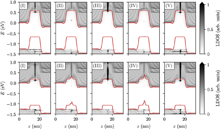
Figure 17. Simulated local density of states of a graphene-nanoribbon FET with a particular defect setup and for different bias positions (top versus bottom). Reprinted by permission from Springer Nature Customer Service Centre GmbH: [Springer Nature] [Journal of Computational Electronics] [320] (2021).
Download figure:
Standard image High-resolution imagePoljak et al conducted a performance study of 15 nm-gate-length MOSFETs based on silicene nanoribbons [321]. The width scaling, series resistance, and transport characteristics were investigated by using an NEGF approach and corresponding silicene nanoribbon Hamiltonians that are expressed in an atomistic tight-binding basis.
Zhang et al studied different designs of vertically stacked horizontal Si and Ge nanosheet GAA pMOSFETs (sub-5 nm node) using an NEGF approach [322]. The ON-state current and subthreshold swing were calculated and evaluated.
Lv et al used quantum dynamics simulations to analyze the electronic fluctuation issue of the so-called armchair graphene nanoribbon MOSFETs [323]. In addition to electron transport, the authors also considered the behavior of the C and H nuclei and used DFT as well as an NEGF transport simulator provided by NanoTCAD ViDES. 6
Tamersit proposed a new double-gate band-to-band tunneling junctionless graphene nanoribbon FET with a sub-10 nm gate length by using a self-consistent Poisson-NEGF simulation approach (in the ballistic limit) [324]. Several key electrical properties, such as the IDS–VGS transfer characteristics, were simulated and discussed. Other work of the author, including colleagues and using a similar simulation approach, focused on investigating a nanoscale coaxial-gate negative-capacitance carbon nanotube FET with a metal–ferroelectric–metal–insulator–semiconductor structure [325].
Abdi et al looked into an optimized design of a textured graphene nanoribbon phototransistor [326]. Here, the graphene layer acts not only as the channel but also as the light absorber. The authors used an NEGF mode-space approach.
Sun et al investigated the operation modes of a dual-gate reconfigurable (silicon-nanowire) FET [327]. Reconfigurable FETs use electrostatic doping for virtual n-/p-regions and can be tuned to operate as unipolar n-/p-transistors. The authors used a self-consistent NEGF approach and solve it one-dimensionally on a finite-difference grid using an effective mass approximation (symmetric conduction and valence band).
7.2. 2D FETs
The staggering advancement of 2D materials (see section 6.1) also triggered substantial research into utilization as channel materials for FETs, collectively named: 2D FETs [328–331].
Selection of recent computational research: Ye et al studied the performance limits of monolayer bismuthane (BiH) transistors considering spin-orbital coupling using a coupled DFT–NEGF approach [332]. The authors particularly focused on the required device width to achieve suitable OFF-state currents.
Kim et al used a computational simulation workflow which also uses a DFT–NEGF approach to investigate the device performance of double-gated silicene/gallium phosphide heterobilayer FETs [333]. The authors could predict that these FETs have attractive characteristics, such as high ON-state current.
Han et al analyzed the photoresponse mechanisms (photoconductive and photogating effects) in MoSe2 transistors [334]. Using a self-consistent simulation approach based on solving the Poisson's equation, an NEGF approach, and considering charge trapping the authors were able to, among others, identify photogating effects as the primary contributor to the overall photocurrent.
Liu et al simulated sub-10 nm double-gate monolayer Cs2PbI4 MOSFETs by using a coupled DFT–NEGF approach [335]. Good subthreshold swing values, ON-state current, and delay time were predicted.
Guo et al studied monolayer α-CS with a puckered structure for potential application as a channel material for sub-5 nm FETs [336]. The authors used a coupled DFT–NEGF approach to calculate the electrical characteristics which yielded attractive results, in particular regarding the ON-current.
Klinkert et al used a coupled DFT–NEGF approach to investigate the orientation misalignments and their impact on the performance of black phosphorus FETs [337]. N- and p-type configurations were investigated including six alignment angles. Ballistic transport as well as electron–phonon and charged impurity scattering was assumed.
Ding et al investigated the ballistic transport performance and gate control mechanism of sub-10 nm monolayer GeS metal-oxide-semiconductor FETs by using a coupled DFT–NEGF approach [338], see figure 18. A particular focus was on evaluating the ON-state current, subthreshold swing, delay time, and power consumption.

Figure 18. Simulated double-gate monolayer GeS MOSFET: calculated local density of states and spectral current densities for different gate biases (top) and transmission eigenstates for different configurations (bottom). Reprinted with permission from [338]. Copyright (2021) American Chemical Society.
Download figure:
Standard image High-resolution imageZhang et al simulated sub-5 nm gate-length double-gate monolayer MoS2 MOSFETs using a coupled DFT–NEGF approach [339]. Based on the results the authors predicted that 1–5 nm gate lengths fail to meet certain expectations (e.g., ON-state current) but with the introduction of a negative capacitance dielectric layer some of them could be mitigated.
Cao et al looked at dissipative transport in antimonene and arsenene double-gate n-type FETs using a coupled DFT–NEGF simulation approach [340]. Among others, the authors highlighted that the ON-current can be highly impacted by optical intravalley and intervalley phonon scatterings and that simulations not properly considering these are seriously overestimating device performance.
7.3. Tunneling FETs
Tunneling FETs (TFETs) differ from conventional FETs by using a different switching mechanism which is based on quantum tunneling through a barrier. For reviews on this topic see, for instance, [341, 342].
Selection of recent computational research: Gnani et al investigated the performance of an inverter based on an n- and p-type TFET considering InAs/Al0.05Ga0.95Sb and interface traps and localized strain [343]. A four-band k ⋅ p Hamiltonian is used in combination with an NEGF approach self-consistently coupled to a Poisson solver.
Ahn et al introduced an advanced NEGF simulation approach to reduce the computational burden of atomistic-level simulations of FETs [344]. The approach is based on using the R-matrix (for details on the R-matrix method see [345]) and recursive Green's function method and was evaluated considering a germanane/InSe vertical tunneling FET.
Brahma et al studied electron–phonon coupling limited transport in phosphorene MOSFETs and TFETs [346]. Among others, the local density of states and spectral current densities were calculated (see figure 19) using hybrid DFT whereas transport is solved by an NEGF approach using a DFT-calibrated two-band k ⋅ p Hamiltonian. Electron–phonon scattering was incorporated. Among others, the authors could show that optical phonon modes are primarily responsible for the degradation of the ON-current.
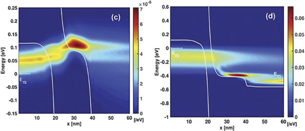
Figure 19. Current spectrum (superimposed on the conduction edge profile) for the considered TFET in the dissipative regime in the OFF-state (left) and ON-state (right). Reprinted from [346], with the permission of AIP Publishing.
Download figure:
Standard image High-resolution imageChen et al proposed an improved design of a triple heterojunction tunneling FET with a 12 nm body thickness based on doping profile engineering [347]. To that end, the authors used a mode-space quantum transport simulation approach, considering thermalization and scattering, to optimize the device design.
7.4. Other types of FETs and diodes
This section collects all remaining FET designs, ranging from the predominant FinFET to ultrahin-body FETs and other types of related devices.
Selection of recent computational research: Pala et al presented a new method for full-band quantum transport simulations based on an empirical pseudopotential Hamiltonian and an NEGF approach [348]. The method was showcased by considering planar, ultrathin-body FETs and nanowire FETs. The authors further discussed different crystal orientations as well as various strain/stress scenarios.
Vyas et al introduced a method based on the Pauli master equation supporting dissipative quantum transport, which keeps the transfer-wave-vector dependence of the scattering processes [349]. A Schrödinger–Poisson solver using the effective-mass approximation was used in the 2D plane of the device. The quantum transmitting boundary method was applied because of open boundary conditions. Finally, dissipative transport was modeled using the Pauli master equation. Ultra-thin body FETs were studied with respect to electron–phonon and surface roughness scattering to evaluate the method.
Kao et al studied the subthreshold swing of source-to-drain tunneling short-channel MOSFETs at cryogenic temperatures [350]. To that end, a coupled Poisson-NEGF simulation approach was employed. The authors discussed four features concerning subthreshold swing saturation dominated by source-to-drain tunneling.
Cam et al coupled Landau–Khalatnikov and Poisson equations self-consistently with the NEGF formalism and used the simulation approach to study ultra-scaled (i.e., to sub-10 nm gate lengths) metal–ferroelectric–insulator–semiconductor negative-capacitance FETs [351]. Based on the simulations, the authors could show that the considered device structure holds attractive properties, e.g., concerning subthreshold slope.
Kumar et al considered a split-gate 2D MoTe2 FET to design an AND gate and studied the device by using an NEGF approach [352]. Back-gate parameter variations were studied with respect to their impact on device performance.
Khaliq et al used doping engineering to improve the electrical characteristics in double-gate pMOSFETs hosting a 5 nm gate length [353]. A NEGF approach was used in combination with a six-band k ⋅ p Hamiltonian.
Damodaran et al investigated a quantum well modulation-doped FET for use as a quantum dot memory device [354]. Their approach centered around a self-consistent Schrödinger–Poisson solver and an eight-band k ⋅ p model. Among others, the results showed that information (i.e., electrons/holes) can be stored longer with increased dot sizes.
Related to FETs are diodes, which contain some form of junction with which to realize the diode functionality. In what follows, a few computational studies are highlighted which explicitly focus on diodes.
Schulz et al introduced a numerical approximation technique for the Wigner transport equation (including the spatial variation of the effective mass) and applied it to simulating a resonant tunneling diode with different material systems using a GaAs/Alx Ga1−x As structure [355], see figure 20.

Figure 20. Snapshot of the simulated evolution of the Wigner function at 500 fs of the considered resonant tunneling diode. Reproduced from [355]. CC BY 4.0.
Download figure:
Standard image High-resolution imageAbedi et al suggested a time-dependent quantum transport model considering elastic scattering and based on the time-dependent Schrödinger equation [356]. Similar to the NEGF approach, an imaginary potential is added to the Schrödinger equation for absorbing electron waves [357]. Also, a source term is added to model the injection of electron waves. Again, a resonant tunneling diode was used to showcase the model.
Dey et al applied a coupled DFT–NEGF approach to study quantum ballistic transport properties of a doped guanine-nanosheet-based bio-Zener diode [358]. Coherent tunneling and incoherent hopping processes are covered by the considered Hamiltonian.
Zhao et al introduced a boron intratube p-i-n junction via gas storage for diode applications [359]. The authors used a coupled DFT–NEGF approach to describe and simulate the electronic structure and transport properties.
8. Quantum cascade devices
QCLs represent prototypical applications of the quantum cascade effect. QCLs have historically been associated with the field of quantum electronics and remain a core research topic in this area. For reviews see, e.g., [360–364].
Selection of recent computational research: Hałdaś et al used an NEGF approach to simulate scattering transport in a THz QCL [365]. The authors developed a non-uniform mesh based approach to tackle the computational effort. A GaAs/AlGaAs material system was considered.
Kolek et al applied the NEGF formalism to calculate the properties of a 5.2 μm wavelength emitting QCL and optimized the device design [366]. Among others, the authors found that the maximum optical power is not exclusively described by the value of the gain peak. In follow-up work, a numerical efficient approach to implement light–matter interactions in NEGF via self-energies [367].
Wang et al also utilized an NEGF approach to study the parasitic paths in two-well scattering-assisted THz QCLs operating at 3.5 THz [368]. These paths are responsible for significantly reducing the efficiency of these devices. Due to their research, the authors were able to suggest approaches to suppress these paths and thus increase efficiency again.
Kato et al studied enhancement of GaInAs/AlInAs mid-infrared QCLs by improving the accuracy of the energy levels [369]. The energy-dependent effective mass of electrons was calculated from the complex band structure of each bulk material of the QCL. The thus calculated effective mass was used in an NEGF approach to compute the lasing wavelength/optical gain peak.
Ushakov et al introduced a balance-equation method for simulating THz QCLs using a wave-function basis [370]. Dephasing was taken into account and the current-voltage and power characteristics were calculated.
Franckié et al applied Bayesian optimization algorithms in combination with an NEGF approach to determine and improve the maximum operating temperature of THz QCLs [371]. The authors argue that their Bayesian optimization approach converges faster and more robustly then a genetic algorithm. Different device designs based on two and three wells per period were considered, including optimal extraction energy and electron–electron correlations.
Gower et al used an NEGF approach to analyze a split-well direct phonon THz QCL (three-level system), offering effective suppression of thermally activated leakage channels [372]. The results clearly highlighted the importance of interface roughness and impurity scattering strengths for device operation. Figure 21 shows the calculated density of states and electron density plots for the considered device.
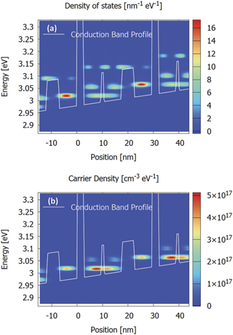
Figure 21. Calculated density of states (top) and electron density (bottom) of the considered split-well direct phonon THz QCL. Reproduced from [372]. CC BY 4.0.
Download figure:
Standard image High-resolution image
Kazemi-Tesieh et al proposed an electrically driven optically excited THz QCL through frequency down-conversion optical nonlinearity [373]. The authors used a self-consistent Schrödinger–Poisson solver to calculate the bandstructure. Also, a density matrix formalism and the energy-density balance equation was applied to provide a self-consistent electro-opto-thermal model considering nonlinearities of the device.
Soleimanikahnoj et al presented a density-matrix approach for mid-infrared QCLs, which is based on a Markovian master equation for the density matrix [374] (Knezevic's group also looked at a Wigner function approach to model dissipative transport [375] and at multi-scale electrothermal simulations [376]). The approach covers in-plane dynamics, preserves positivity of the density matrix, and does not rely on phenomenologically introduced dephasing times. A three-band k ⋅ p model is used to account for the nonparabolicity in the band structure. This work was extended to study photon-assisted electron transport [377].
9. Heat transfer and thermoelectric systems
Until now we focused on electron transport and/or on electric structure properties. What we have omitted so far is a discussion on heat transfer and potential thermoelectric effects which accompanies electron transport. For more background on this topic, the reader is referred to [238, 279, 378, 379].
Selection of recent computational research: Chu et al used an NEGF approach with Büttiker probe scattering self-energies to calculate the thermal boundary resistance of an Si/heavy–Si-interface (heavy-Si differs from Si in its atomic mass ratio) and compared it to molecular dynamics simulations [380].
Foster et al investigated the impact of nanoinclusions and voids on the electronic and thermoelectric coefficients of 2D nanocomposites using an NEGF approach [381]. The modeling approach considered geometry, electron–phonon interactions, quantization, tunneling, and the ballistic-to-diffusive nature of the transport.
Slimane et al introduced a gauge-invariant theoretical framework which allows to describe time-resolved thermoelectric transport in an arbitrary multi-terminal electronic quantum system described by a noninteracting tight-binding model [382]. Driven, non-equilibrium conditions are considered, e.g., an external time-dependent electromagnetic field. The authors extended the wave-function approach of Gaury [119] by including energy transport and implemented their approach in the TKWANT library [75]. A simulation of dynamical thermal transport in a quantum point contact subjected to voltage pulses was used as a showcase.
Crépieux calculated heat current fluctuations in a quantum dot coupled to electron reservoirs at finite frequency, voltage, and temperature using an NEGF approach [383]. Among others, the link between the asymmetry of the quantum dot-reservoir couplings was studied as well as the heat noise for a (non-)equilibrium quantum dot.
Knezevic discussed a multi-scale electrothermal simulation approach for QCLs with a focus on describing the highly nonequilibrium physics of the embedded strongly coupled electron and phonon systems [376]. In earlier work, the thermal conductivity of ternary III–V semiconductor alloys and the role of mass difference and long-range order was investigated using equilibrium molecular dynamics [384].
Foss and Aksamija used first-principles calculations and phonon interface transport modeling to calculate the temperature-dependent thermal boundary conductance in single layers of several 2D materials, e.g., silicene, hBN, boron arsenide, and blue and black phosphorene [385]. In related work on 2D materials, the group looked at electrical and electrothermal properties of few-layer 2D devices [386]. In previous work, the group used the Wigner–Rode formalism to investigate the impact of potential barrier geometries (applied to a single layer of MoS2) on transport [387] and to study the thermoelectric properties of periodic quantum structures [388].
10. Summary and outlook
In many areas of science and engineering, computational tools have matured to a degree where computational experiments are a reality and a necessity. Combined with the broad availability of large-scale parallel computing resources, computational tools enable us to not only increase our understanding of fundamental physical processes and properties, but most excitingly to predict and design a plethora of quantum electronic devices and systems. Quantum electronics and its extended focus on utilizing the wave nature of electrons profoundly benefits from these developments as can be seen from the plethora of research published just in the highlighted focus areas of the last years alone. This development will continue and computational tools will further increase in importance to advance research and development in the many focus areas of quantum electronics.
What is particularly exciting is the extensive inter-disciplinarity of quantum electronics today. From QCLs and other nanoelectronic devices, such as the various flavours of FETs and heat transfer based devices, to material and superconducting systems, electron quantum optics, and finally to different solid-state quantum information processing approaches. Consequently, the research originates from various fields of science and engineering, such as electrical engineering, solid-state physics, chemistry, materials science, applied mathematicians, and computational scientists.
Looking ahead, computational methods will of course need to further evolve. The primary challenge is to reduce simulation runtimes to practical levels, in particular, when considering engineering workflows. Already many tools involve high degrees of parallelization approaches to stem the burden. However, a profound potential for accelerating simulations across the board is promised by machine learning and we will thus see an increased share of research into these directions.
Overall, the computational quantum electronics future is bright.
Acknowledgments
The financial support by the Austrian Science Fund (FWF): P33609 and P33151, the Austrian Federal Ministry for Digital and Economic Affairs, the National Foundation for Research, Technology and Development, and the Christian Doppler Research Association is gratefully acknowledged.
Data availability statement
No new data were created or analysed in this study.
Footnotes
- 3
- 4
- 5
However, classical descriptions served us for a long time and to a considerable degree continue to do so [11].
- 6