

Abstract
An efficient surface defect passivation is observed by reacting clean Si in a dilute hydrogen sulfide–argon gas mixture (<5% H2S in Ar) for both n-type and p-type Si wafers with planar and textured surfaces. Surface recombination velocities of 1.5 and 8 cm s−1 are achieved on n-type and p-type Si wafers, respectively, at an optimum reaction temperature of 550 °C that are comparable to the best surface passivation quality used in high efficiency Si solar cells. Surface chemical analysis using x-ray photoelectron spectroscopy shows that sulfur is primarily bonded in a sulfide environment, and synchrotron-based soft x-ray emission spectroscopy of the adsorbed sulfur atoms suggests the formation of S–Si bonds. The sulfur surface passivation layer is unstable in air, attributed to surface oxide formation and a simultaneous decrease of sulfide bonds. However, the passivation can be stabilized by a low-temperature (300 °C) deposited amorphous silicon nitride (a-Si:NX:H) capping layer.
Export citation and abstract BibTeX RIS
1. Introduction
The termination of silicon (Si) surface dangling bonds is of paramount importance for many electronic and optoelectronic devices. Effective termination of Si surface defects, commonly known as 'Si surface passivation', minimizes trap-assisted recombination in Si solar cells. This minimization of minority carrier recombination at the Si surface, necessary for high open circuit voltage (VOC), is the primary reason for the rapid improvement of Si solar cell efficiency in the last few years, with efficiencies >25% achieved by judicial choice of improved surface passivation layers and device design [1–3]. Furthermore, surface passivation is becoming increasingly important with the manufacturing development of thinner industrial Czochralski (Cz)-grown Si wafers with fewer bulk defects. Record Si solar cell efficiencies of 26.6% in interdigitated back contact Si heterojunction (IBC-SHJ) [4] and 25.7% in both-side contacted tunnel oxide passivating contact (TOPCon) [5] structures are primarily achieved by excellent surface passivation, resulting in high open circuit voltages (VOC ⩾ 725 mV). These advanced cell structures adeptly utilize surface defect passivation of undiffused Si surfaces by thin intrinsic amorphous silicon (a-Si:H) in Si heterojunction (SHJ) [1, 2, 4], and silicon dioxide (SiO2) and polysilicon in TOPCon solar cells [5]. The a-Si:H passivation of SHJ degrades at high temperature and thus limits the downstream cell processing temperature to <300 °C. Additionally, efficient light absorption of a-Si:H layers introduces optical losses when used as a front surface passivation layer [6]. On the other hand, SiO2 passivation layers grown by dry oxidation or wet steam oxidation [7, 8] at high temperature (>850 °C) represent the most common and widely used methods in Si PV, but introduce challenges to maintaining high bulk quality. Therefore, many other alternative oxide-based passivation layers have been investigated extensively over the past decade and are succinctly summarized in a literature review [9].
Sulfur-based passivation layers are, in contrast, studied far less extensively. The Si surface chemistry with H2S has shown similar facile reaction with Si(100) dangling bonds to its analogue H2O [10, 11]. First principle calculations identify that sulfur (S) and selenium (Se) both could restore the Si(100) surface to their ideal bulk-terminated geometry, with a Si–S–Si or Si–Se–Si configuration and the former calculated to induce larger compressive stress by a factor of 3 [12]. Experimentally, hydrogen sulfide (H2S) gas exposure to Si(100) surfaces in an ultra-high vacuum (base pressure ∼4 × 10⁻¹¹ Torr) chamber is shown to result in dissociative adsorption (H2S → H + HS) at temperatures ranging from −145 to 425 °C [13]. Temperature-programmed desorption (TPD) and Auger electron spectroscopy (AES) measurements show a simultaneous desorption of hydrogen, accompanied by S diffusion into the Si crystal over the temperature range 525 °C–625 °C and the formation of Si–S–Si bonds by breaking the Si dimer bonds. N-type and p-type Si(100) wafers are reacted in gas mixtures of hydrogen, HCl, and H2S at 750 °C in a chemical vapor deposition (CVD) system and characterized with Al Schottky contacts [14]. A low barrier height of <0.078 eV on n-type and high barrier height of >0.77 eV on p-type Si is argued to be due to a reduction of surface states by S passivation of Si surfaces. More direct evidence of Si surface passivation by H2S gas phase reaction is reported with a minority carrier lifetime >2000 μs for n-type [15] and >250 μs for p-type Si(100) planar wafers [16].
In this paper, a detailed study of n- and p-type Si surface passivation is presented with varying H2S reaction process parameters, and characterized for electrical performance by surface recombination velocity (SRV) and surface chemical analysis by x-ray photoelectron spectroscopy (XPS) and synchrotron-based soft x-ray emission spectroscopy (XES). The atmospheric and thermal stability of S-passivated Si samples is also investigated.
2. Experiment
In this work, two different types of n-type Cz-grown Si wafers with slightly different thickness (140 and 160 μm) and one type of p-type Cz Si wafer (160 μm) are used to study the passivation process by H2S gas-phase reaction. The n-type wafers with thickness of 140 and 160 μm are henceforth labeled as n1-type and n2-type, respectively. Both n-type and p-type wafers have similar resistivities in the range of 2–5 Ω cm, but n1-and n2-type wafers have different bulk lifetimes, as shown below. The wafers were planarized or textured by etching in potassium hydroxide (KOH) solution, depending on the KOH concentration. The wafer surfaces were then cleaned to remove any residual impurities by a sequence of acid cleaning steps in hydrofluoric acid (HF)–sulfuric acid (H2SO4)–hydrochloric acid (HCl), with a deionized (DI) water rinse in-between every step. After these impurity-removal steps, the wafers were further etched and cleaned in a 1:100 mixture of HF and nitric acid (HNO3), followed by surface-oxide removal in 10% HF for 1 min, as established for high-efficiency SHJ solar cells [17].
The cleaned wafers of 1"× 1" size were immediately loaded into a custom-built quartz tube (2" diameter) CVD reactor [18] and pumped to below 1 × 10⁻⁶ Torr. The wafers were then reacted in a H2S–Ar gas mixture, with an H2S gas-phase concentration from 0 to 13%, at temperatures from 400 to 650 °C, and for a duration from 5 to 210 min. It is to be noted that the H2S gas purity used in this study is 99.9%, with primary impurities consisting of carbon dioxide (CO2), H2O, and hydrocarbons. In our set-up, a heating jacket surrounding the quartz tube heats the samples, and a sheathed K-type thermocouple placed inside the tube and under the samples is used to monitor and control the reaction temperature. The Si wafers are placed vertically in a graphite boat that allows surface passivation on both surfaces simultaneously.
The reactor was filled with Ar gas with a flow rate of 1290 sccm, and the exhaust valve was left open to establish the reactor pressure to 1 atmospheric pressure (760 Torr) at room temperature. The temperature was then ramped up to the desired set point reaction temperature. The appropriate H2S gas flow started when the sample temperature reached 300 °C. After completion of the reaction, the H2S gas flow was stopped when the reactor cooled down to 300 °C and, and the Ar flow continued until the temperature reached room temperature.
The surface passivation quality was evaluated by minority carrier lifetime measurements with a Sinton WCT-100 tool using the quasi-steady-state photoconductance (QSSPC) method [19, 20] on the wafers with S passivation right after their removal from the reactor. In QSSPC, the effective minority carrier lifetime (τeff) at an excess carrier density (Δn) of 1 × 1015 cm−3 and τfit from (1/τeff-Auger term) vs Δn curves are recorded. The SRV values at Δn = 1 × 1015 cm−3 are then estimated using equation (1), with known wafer thickness (W) and assuming τbulk = τfit.

The evolution in SRV over time in atmosphere is monitored by repetitive QSSPC measurements. An 85 nm thick a-SiNX :H layer was also deposited by a radio frequency (13.56 MHz) plasma CVD process at 300 and 350 °C on selected S-passivated samples. These stack-passivated samples were exposed to thermal firing in a belt furnace at ∼750 °C for ∼5 s to verify their thermal stability under industry standard solar cell metallization firing conditions.
The surface and surface-near bulk chemical structures [21, 22] were studied on selected wafer samples by XPS, using Mg Kα excitation and a SPECS PHOIBOS 150 DLD electron analyzer at the University of Nevada, Las Vegas (UNLV), and XES at beamline 8.0.1. of the advanced light source (ALS), Lawrence Berkeley National Lab, using the SALSA endstation [23, 24], respectively. For this purpose, the samples were sealed in a dry-nitrogen containing environment at the University of Delaware (UDel) with minimal air exposure, and shipped to UNLV. The packaged samples were then transferred into a dry-nitrogen filled glovebox and cut into smaller samples. Half of the samples remained at UNLV for XPS measurements, while the other half was subsequently re-sealed and shipped to the ALS in Berkeley without any further exposure to air. Samples were introduced into ultra-high vacuum characterization chambers without (UNLV) or with only minimal (ALS) air exposure. To study the degradation of sulfur-passivated sample surfaces, some samples were stored in air for 8 d at UDel prior to shipment to UNLV.
3. Results and discussion
3.1. SRV values after H2S reaction on n- and p-type planar Si wafers
As shown in equation (1), the SRV values can be calculated from τeff, if the τbulk and wafer thickness are known. To validate the assumption that τbulk can be assumed to be the τfit estimated from (1/τeff-Auger term) vs Δn curves, τfit values are recorded with varying τeff obtained by different passivation processes. If the H2S reaction passivates only the surface defects and the surface degrades under air exposure without affecting bulk lifetimes, the τbulk and hence τfit will be independent of τeff. Figure 1 shows the estimated τfit for three types of wafers, indicating a range of surface passivation quality obtained after H2S reaction at different process conditions and during the atmospheric degradation with different τeff. Clearly, τfit is found to be independent of the surface passivation quality, and therefore determined to be representative of τbulk of the respective wafers. Average τfit of 10 000 μs, 4000 μs and 400 μs are obtained for n1-, n2-, and p-type wafers, respectively. These τfit values also closely match the values obtained by state-of-the-art thermal SiO2 and Al2O3 surface passivation structures (symmetric passivation on both surfaces) in n2 and p-type sister wafers from the same batch, and are depicted as 'star symbols' in figure 1.

Figure 1. Estimated τfit at different surface passivation levels (τeff), as measured by QSSPC of n1-, n2-and p-type Si wafers. The star symbols represent Si surface passivated by state-of-the-art thermal SiO2/a-SiNX :H for n2-type and Al2O3/a-SiNX :H for p-type wafers, respectively. The dashed lines are a guide to the eye.
Download figure:
Standard image High-resolution imageFigure 2 shows the SRV values calculated from τeff at Δn = 1×1015 cm−3 and assuming τfit = τbulk using equation (1) for varying H2S reaction temperature (figure 2(a)), H2S concentration (figure 2(b)) in Ar, and time (figure 2(c)). The figure shows that SRV < 10 cm s−1 is achieved at reaction temperatures between 500 °C–650 °C, H2S concentration >1% and for all reaction times between 5–210 min for n-type Si. The lowest SRV ≈ 1.5 cm s−1 on both n1-and n2-type Si is achieved at an optimum temperature of 550 °C, 3.4% H2S concentration with 30 min reaction time. A similar trend of SRV with H2S reaction temperature-concentration-time is observed for p-type wafers, but the SRV values of p-type wafers are higher, presumably due to much inferior bulk quality. Nonetheless, the lowest SRV = 8 cm s−1 is obtained with an optimal reaction process of 550 °C, 3.4% H2S concentration, and 30 min reaction time. The S-passivated Si SRV of 1.5 cm s−1 on n2-type Cz wafer is comparable to the best surface passivation qualities using state-of-the-art materials, SiO2 (2.4 cm s−1), a-SiNX :H (3.5 cm s−1), a-Si:H (0.7 cm s−1), and Al2O3 (1.3 cm s−1), reported in literature [9]. A direct comparison of SRVs obtained by different groups and with different materials could be misleading, since these values can vary appreciably depending on the wafer type, dopant type & concentration (bulk resistivity), wafer manufacturing process (float zone or Czochralski method), and bulk qualities. Therefore, surface passivation by a SiO2/a-SiNX :H stack on n2-type and an Al2O3/a-SiNX :H stack on p-type sister wafers from the same batch was also performed in this work. The τeff and τfit are shown as star symbols in figure 1. The calculated SRV values of 2.7 and 13 cm s−1 for n2-type and p-type, respectively, by the oxide materials are slightly higher (i.e. indicating a poorer passivation) than the best SRV of S-passivated Si (1.5 and 8 cm s−1 for the respective wafer types).

Figure 2. SRV calculated from QSSPC for n1-(square), n2-(circle) and p-(diamond) type Si wafers after passivating both surfaces by H2S at different (a) temperatures; (b) H2S concentrations in Ar; and (c) reaction durations. For each process parameter variation, the other two parameters are kept constant, as defined in each plot. The τeff values are measured immediately after the samples were taken out from the passivation reactor. The dashed lines are guides to the eye.
Download figure:
Standard image High-resolution imageA continuous decrease in SRV, up to reaction temperatures =550 °C, suggests that the hydrogen atoms are likely not responsible for the surface passivation in this process, since hydrogen desorbs from the surface in the temperature range of 400 °C–550 °C [13]. Interestingly, an increase of surface S/Si ratio in AES is reported up to a temperature of 550 °C, followed by a sharp decrease in sulfur (S) peak intensity for temperatures >625 °C [13]. This loss of S-signal was initially attributed to desorption of S from the surface [25], but it was then argued to be due to S-diffusion into the Si bulk, since no S was detected in TPD measurements [13]. Furthermore, low-energy electron diffraction studies of S adsorption on clean Si(100) surface indicated that S adsorbates can cause a transition of the reconstructed Si(100)2 × 1 surface to its original bulk-terminated Si(100)1 × 1 structure [26–28]. Thus, considering the results reported in literature, a plausible explanation for the efficient surface defect passivation (low SRV), observed in this study in the temperature range of 550 °C–600 °C, is based on a S-induced Si(100)2 × 1 surface reconstruction to the original bulk-terminated Si(100)1 × 1 surface by breaking the Si dimer bond [13, 25]. At higher temperatures (650 °C), S atoms may diffuse to the near-surface Si bulk and create additional defects generated by sub-surface S–Si bonds leading to higher SRV, especially evident for p-type Si in figure 2(a). A small dose of H2S (<1% in Ar) in the reaction process at 550 °C for 30 min is sufficient to reduce SRV by ∼2 orders of magnitude for both n-type and p-type Si, but no surface passivation is observed without the H2S (figure 2(b)). This suggests that the surface passivation is determined by an extremely thin, likely ∼(sub)monolayer coverage of S. Finally, a constant low SRV for 3.4% H2S at 550 °C in the entire range of reaction duration (5–210 min) (figure 2(c)) indicates a fast process for efficient surface passivation.
3.2. SRV comparison of S-passivation on planar and textured Si wafers
In order to apply this novel S-passivation approach to any Si solar cell structure, it is imperative to demonstrate efficient surface passivation (low SRV) on textured surfaces. The front illumination surface of a Si solar cell needs to be textured for low optical reflection loss. In this study, n2-type Si wafers were etched in dilute KOH solution to create a random pyramid structure that increases the surface area and forms {111} facets on the Si(100) surface. Figure 3 shows the SRV comparison for planar and textured n2-type Si wafers after H2S reaction at 550 °C in varying concentration (figure 3(a)) and time (figure 3(b)). Figure 3 demonstrates that both planar and textured surfaces are passivated equally well. Therefore, the same passivation mechanism is valid for both planar and textured wafers with a fast defect-terminating process, despite the increase in area of the {111} faceted surface in textured Si.

Figure 3. SRV of planar (circle) and textured (triangle) n2-type Si wafers after H2S passivation at 550 °C and at different (a) H2S concentrations; and (b) reaction durations.
Download figure:
Standard image High-resolution image3.3. Atmospheric and thermal stability of SRV after H2S reaction
Atmospheric stability of S-passivated planar Si wafers is evaluated after exposure in laboratory air at relative humidity of 40%–60% for an extended period of time. Figure 4 shows that the passivation quality degrades rapidly as a function of time in air, SRV increases by ∼an order of magnitude within 30 min. The degradation rate is similar for both n- and p-type wafers, despite the difference in their initial SRV. This rapid loss of surface passivation is explained by a change of S–Si surface bonds to form SiO2 in a thin (<5 nm) S surface layer, as reported for similar H2S reaction conditions [15]. The resulting low temperature native oxide does not passivate Si surfaces well on its own [9]. Furthermore, loss of Si surface passivation by ultrathin layers is not surprising and is also observed for Si surfaces passivated by ultrathin (<5 nm) a-Si:H [29], Al2O3 [30, 31] and SiO2 [32].
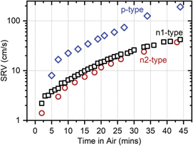
Figure 4. Degradation of passivation quality (increase of SRV) in ambient laboratory air after H2S passivation at 550 °C in 3.4% H2S for 30 min of n1-(square), n2-(circle) and p-(diamond) type Si wafers.
Download figure:
Standard image High-resolution imageA simple mitigation strategy to eliminate the passivation degradation can be achieved by capping the S-passivated surface using a low-temperature-deposited thin a-SiNX :H films. A set of wafers were passivated by 3.4% H2S reaction at 550 °C for 30 min in multiple runs, and the samples were immediately loaded into a PECVD reactor for a-SiNX :H deposition. The air exposure of the S-passivated samples during transfer between the two systems was <5 min. A 85 nm layer of a-SiNX :H was deposited on both sides of the S-passivated samples at 300 °C to protect the S-layer from air exposure. Freshly cleaned wafers without the S-passivation were also included in each a-SiNX :H deposition run, for comparison. The SRV's of the samples were recorded by repetitive QSSPC measurements for up to ∼2 months, with samples stored in laboratory air. Figure 5 shows the change in SRV as a function of time for n2-type and p-type wafers with and without the S-passivation layer. The initial SRV was 5 cm s−1 for n2-type Si, passivated by a S + a-SiNX :H stack, which remained stable for months with no degradation. However, a slow degradation of SRV from 8 to ∼20 cm s−1 over 2 months storage in air is observed for the p-type wafer passivated by the same stack layer. This difference in SRV stability between n2-type and p-type Si is not well understood and requires further investigation. Nonetheless, a low-temperature a-SiNX :H capping layer effectively slows down the SRV degradation rate and stabilizes SRV for months, as opposed to a rapid SRV degradation (an order of magnitude in 30 min) observed in figure 4 without the capping layer. Such low-temperature a-SiNX :H alone, however, does not provide any significant surface passivation, with SRV > 600 cm s−1 (figure 5), which was also observed in our previous work [15, 33]. We note that the a-SiNX :H layer can also be used as an antireflection coating by controlling the thickness and the refractive index [34].

Figure 5. Change in SRV with storage time in air, up to ∼65 d, followed by a thermal firing step on day 90 for n-type and p-type Si, surface-passivated by a S + a-SiNX :H stack and a-SiNX :H layers. The shaded region lists the thermal firing temperature and time in a standard Si cell metallization belt furnace. The dashed lines are guides to the eye.
Download figure:
Standard image High-resolution imageIn order to further investigate the thermal stability of S + a-SiNX :H stack passivation, the samples were subjected to thermal firing at peak temperature ∼750 °C for ∼5 s. Figure 5 shows that SRV after thermal firing on day 90 increases from 5 cm s−1 to ∼30 cm s−1 for n2-type and 30 cm s−1 to ∼300 cm s−1 for p-type Si. Therefore, the passivation loss is evident for both types of wafers upon thermal treatment, but the SRV values are still ∼an order of magnitude lower than the samples that did not have any S-passivation and were coated with low-temperature a-SiNX :H only. The wafers passivated by only a-SiNX :H do not show any changes in SRV upon thermal firing, albeit at a much higher values of >600 cm s−1. A careful examination of surface morphologies before and after the thermal firing step for both a-SiNX :H and S + a-SiNX :H passivated Si surfaces reveals an appearance of blistering and pinholes upon thermal firing. Surface blistering is likely due to the desorption of molecular hydrogen (H2) from the unoptimized low-temperature deposited a-SiNX :H films, with a low film density as reported in literature [35]. These pinholes can lead to pathways for atmospheric oxidation of the S-layer underneath the a-SiNX :H and cause fast SRV degradation, as in figure 4.
Further process optimization of a-SiNX :H capping layers does, in fact, eliminate the thermal degradation of S + a-SiNX :H stack passivation. A set of emitter-diffused Si wafer samples was passivated by H2S reaction to achieve an emitter saturation current density (J0e) < 70 fA cm−2 and τeff > 600 μs. The S-passivated wafer surfaces were then protected on both-sides by an (unoptimized) 30 nm thick low-temperature (300 °C) deposited a-SiNX :H at UDel, followed by a 70 nm a-SiNX :H layer deposited at 425 °C, optimized for industrial Si solar cell processes, at Georgia Institute of Technology. The emitter saturation current densities (J0e) and τeff of these stack-passivated samples remain stable, with no visible surface blistering and pinholes, after the same thermal firing step (∼750 °C for ∼5 s). This demonstrates that an ultrathin S-layer, in combination with an optimum a-SiNX :H process, can indeed achieve atmospheric and thermally stable excellent surface passivation for both n- and p-type Si. Details of the dopant-diffused Si surface passivation by S and the mechanism for thermal stability is, however, beyond the scope of this paper and will be reported in a future publication.
3.4. Surface chemical studies of S-passivated Si by photoelectron and soft x-ray spectroscopies
The chemical environment at the surface and surface-near bulk of the n1-type Si wafers were investigated using XPS and XES. Figure 6 shows the XPS detail regions of S 2s (a) and Si 2p (b) after the HF cleaning process prior to H2S reaction ('clean'), after the H2S reaction ('passivated'), and after 8 d of air exposure ('degraded'). The gray boxes represent binding energies commonly found for the various chemical environments, namely, sulfur in a S–O and sulfide chemical environment, and silicon in Si–Si and Si–O bonding environments. No Si–O bonds are present on the 'clean' Si wafer surface, indicating the effectiveness of the cleaning process and packing procedure. Note that a small amount of sulfur in a sulfide chemical environment is already present at the surface of the 'clean' wafer (at a binding energy of ∼226.5 eV), presumably due to sulfur in the cleaning process. After the H2S passivation reaction, the S 2s spectra show sulfur mainly in a sulfide environment, with a small sulfur signal representative of a S–O environment (binding energy ∼233 eV). After exposure to air (i.e. for the 'degraded' sample), the sulfur signal in the spectrum decreases, but remains in a sulfide chemical environment. This is attributed to a loss of sulfur during air exposure of the surface, e.g. interacting with moisture in the air. Likely, H2S is formed and desorbed, allowing Si–O bonds to form instead [15, 36]. As evidence, the Si–O bond signal in the Si 2p core levels increases (and is dominant) after exposure to air, with a decrease in Si–Si bonds. Note that, already during the passivation reaction, some Si–O bonds are formed but Si–Si bonds remain dominant. The degradation processes then reverse this balance at the Si wafer surface; similar findings with different wafer types were also reported previously [16]. The likely source of the Si–O peak in the passivated samples is argued to be due to impurities in 99.9% H2S source gas itself, since similar time-temperature reactions performed in the same reactor with 99.999% purity Ar with no H2S gas flow only found negligible Si–O peaks in XPS [15]. The manufacturer certificate of analysis of 99.9% H2S indicated that as much as 500 ppm of water vapor is present in the H2S source gas. A higher purity H2S source gas and/or additional in-line gas purifier would be needed to minimize/eliminate the presence of a Si–O XPS peak in the passivated samples.
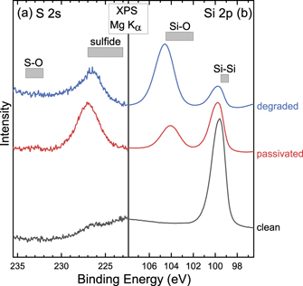
Figure 6. Mg Kα XPS spectra of (a) S 2s and (b) Si 2p detail regions of the n1-type Si wafers: cleaned, passivated, and degraded. Gray bars indicate regions dominated by specific bonding environments.
Download figure:
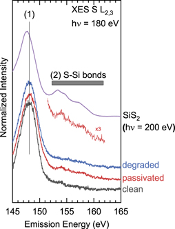
Standard image High-resolution imageUsing S L2,3 XES, the local chemical bonding environment of sulfur at the surface and in the surface-near bulk can be studied in a complementary approach to XPS. Figure 7 shows the S L2,3 emission of the three samples, together with a SiS2 reference powder and a magnified section of the 'passivated' spectrum' to better identify the chemical fingerprint of S–Si bonds (note that the SiS2 powder sample was scanned under the x-ray beam to avoid beam damage). All spectra in figure 7 were normalized to the maximum count rate of the spectrum, i.e. at the S 3s-derived emission line labeled (1). The presence of this peak indicates sulfur atoms in a sulfide environment. As for XPS, the 'clean' spectrum already shows some sulfur in a sulfide chemical environment. After the passivation process, (further) S–Si bond formation can be seen through the spectral features between 152 eV to 160 eV (also shown enlarged (×3) to compare with the SiS2 spectrum). However, after air exposure (i.e. in the 'degraded' spectrum), these features are no longer present. This indicates the removal of S–Si surface bonds after air exposure and corroborates the decrease in XPS sulfur intensity. Overall, both XPS and XES studies thus show a reduction of S–Si bonds and the formation of Si–O bonds due to air exposure, in parallel to the observed increase in SRV.
Figure 7. S L2,3 XES spectra of three n1-type Si wafers (cleaned, passivated, degraded) and a SiS2 reference. A magnified (×3) section of the 'passivated' spectrum is also shown. (1) Indicates S 3s-derived signals of a sulfide environment, (2) labels the upper valence band region of SiS2 (indicative of S–Si bonds).
Download figure:
Standard image High-resolution image
4. Conclusions
The reaction of clean Si wafers in H2S gas at temperatures between 550 and 600 °C provides excellent surface passivation for both n-type and p-type c-Si with planar and textured surfaces. SRV values of 1.5 and 8 cm s−1 are achieved on n-type and p-type Si, respectively, by reacting Si wafers in a 3.4% H2S–Ar gas mixture for 30 min. Efficient surface passivation is observed for reaction times as short as 5 min, and H2S concentrations as low as 1%. We conclude that the low SRV is a result of Si surface restructuring that minimizes surface defect state densities. The fast SRV degradation in air suggest that the S-passivated layer is extremely thin and readily reacts with atmospheric moisture and oxygen. Such air degradation can be eliminated by applying an a-SiNX :H capping layer; however, the a-SiNX :H process requires optimization to achieve the desired thermal stability. We infer that the H2S reaction process with Si wafers can be described as a three-step process: (1) a dissociative adsorption of H2S (H + HS and H2 + S) to Si, (2) surface restructuring to an ideal bulk-terminated Si by breaking Si dimer bonds with minimum surface dangling bonds/defects, and (3) S-diffusion to the near-surface bulk, depending on reaction temperature and time.
Legal disclaimer
This report was prepared as an account of work sponsored by an agency of the United States Government. Neither the United States Government nor any agency thereof, nor any of their employees, makes any warranty, express or implied, or assumes any legal liability or responsibility for the accuracy, completeness, or usefulness of any information, apparatus, product, or process disclosed, or represents that its use would not infringe privately owned rights. Reference herein to any specific commercial product, process, or service by trade name, trademark, manufacturer, or otherwise does not necessarily constitute or imply its endorsement, recommendation, or favoring by the United States Government or any agency thereof. The views and opinions of authors expressed herein do not necessarily state or reflect those of the United States Government or any agency thereof.
Acknowledgments
Authors thank Professor William Shafarman of Institute of Energy Conversion for many helpful discussions about surface reactions by hydrogen sulfide. This work is supported by the US Department of Energy's Office of Energy Efficiency and Renewable Energy (EERE) under Solar Energy Technologies Office (SETO) Agreement Number DE-EE0008554. The synchrotron-based research of this study used resources of the Advanced Light Source, a US DOE Office of Science User Facility under Contract No. DE-AC02-05CH11231.
Data availability statement
The data that support the findings of this study are available upon reasonable request from the authors.