

Abstract
Using relativistic density-functional calculations, we examine the magneto-crystalline anisotropy and exchange properties of transition-metal atoms adsorbed on 2D-GaAs. We show that single Mn and Mo atom (Co and Os) strongly bind on 2D-GaAs, and induce local out-of-plane (in-plane) magnetic anisotropy. When a pair of TM atoms is adsorbed on 2D-GaAs in a close range from each other, magnetisation properties change (become tunable) with respect to concentrations and ordering of the adatoms. In all cases, we reveal presence of strong Dzyaloshinskii–Moriya interaction. These results indicate novel pathways towards two-dimensional chiral magnetic materials by design, tailored for desired applications in magneto-electronics.
Export citation and abstract BibTeX RIS
1. Introduction
Two-dimensional (2D) materials are nowadays being intensely studied both theoretically and experimentally due to their unique physical properties [1–8]. Most of them are nonmagnetic in their pristine form, which restricts their applications in magneto-electronics. According to the Mermin–Wagner–Hohenberg theorem [9, 10], thermal fluctuations strongly suppress long-range magnetic order in two-dimensional materials at any non-zero temperature, even if those materials are intrinsically magnetic in 3D bulk form; nonetheless, such detrimental effect of fluctuations can be neutralized by presence of magnetic anisotropy (MA). The pioneering experimental confirmations of magnetism in CrI3 [11] and CrGeTe3 [12] in 2017 opened an entirely new field of atomically-thin magnetic crystals, that does not cease to surprise [13]. For example, the critical temperature of CrGeTe3 tends to zero when material is reduced in thickness to the monolayer limit. However, when anisotropy is introduced in the CrGeTe3 system, by application of an (even tiny) external magnetic field, a non-zero magnetisation establishes at finite temperature [12, 13]. Zhang et al reported robust intrinsic ferromagnetism and half semi-conductivity in two-dimensional single-layer chromium trihalides. They found a magnetocrystalline anisotropy energy (MAE) of 685.5 μeV and 185.5 μeV for 2D-CrI3 and 2D-CrB3 [14], respectively. The authors state that 2D-chromium trihalides systems are promising candidates for low-dimensional magneto-electronic applications. For comparison, these values of MAE are higher than those found for ferromagnetic materials such as bulk Fe, Ni and Co, which present a MAE per atom of 1.4 μeV, 2.7 μeV and 65 μeV [15], but lower for transition metal monolayers [16], magnetic atoms on metal surface [17] and ferromagnetic–semiconductor interface [18], whose MAE per atom are on the order of meV.
The spin–orbit coupling (SOC) is the microscopic source of MA. Hence, tuning the orbital and spin moment of a crystal is fundamental; as an illustration, the MA in a 2D material can be induced by doping with transition metals, among other ways of manipulating the SOC of a crystal [19–22]. Long-range ferromagnetic ordering and high MA have been found in manganese-doped 2D systems [14, 23, 24]. Using density functional theory (DFT) calculations, Mishra et al reported long-range ferromagnetic ordering in Mn-doped two-dimensional dichalcogenides [23]. Sun et al demonstrated that the MnX3 (X = F, Cl, Br, I) are dynamically and thermodynamically stable up to high temperatures, and exhibit large magnetic moments (4 μB), high Curie temperatures, and large in-plane MA energies [24].
On the other hand, diluted magnetic semiconductors based on III–V group materials have been of great interest in 3D systems due to their potential applications in spintronic devices [25–29]; in particular bulk Mn-doped GaAs has attracted significant interest in that respect [27–29]. The question arises: how the MA properties of the Mn–GaAs system evolve in the ultrathin limit of that material? Lan et al investigated from first principles the magnetic properties of 2D (Ga, Mn)As but did not study the MA of this material, nor covered the magnetic exchange in sufficient detail [30].
Recent theoretical [22, 31] and experimental [32] works have reported that the adsorption or doping of Os and Co on/in 2D monolayer systems can induce a large MA. Sivek et al showed by an ab initio study that transition-metal atoms (Os and Co) adsorbed on MoS2 and fluorographene monolayers can cause a huge magnetocrystalline anisotropy to arise [31]. Furthermore, Torun et al found a high MAE in Co on graphene and Os-doped MoTe2. They reported an out-of-plane and in-plane easy-axis direction of Co-on-graphene and Os-doped MoTe2 systems, respectively [22].
Another important consequence of relativistic effects i.e., SOC combined with a broken spatial inversion symmetry, is the appearance of Dzyaloshinskii–Moriya interaction (DMI) [33, 34]. DMI, characterized by a Dzyaloshinskii–Moriya vector D acting on a pair of spins, is an antisymmetric magnetic exchange interaction that aligns the neighbouring spins orthogonally to each other, with a unique sense of rotation, instead of the parallel or antiparallel spin alignments obtained by the usual Heisenberg exchange interaction [35]. DMI is essential for creating non-collinear long-range spin order in ultra-thin magnetic films, and is responsible in the creation, stabilisation and manipulation of skyrmions and chiral domain walls as bearers of attractive applications in novel spintronic, memory and logic devices [36, 37]. Thin-film heterostructures consisting of transition metal layers have been investigated on the basis of first-principles calculations in combination with spin-polarised scanning tunnelling microscopy, to report how DMI influences their magnetic structure, and changes standard perception of magnetic properties [38–41].
Motivated by above developments, and by recent theoretical reports about the dynamical and mechanical stability of 2D-GaAs semiconductor [5, 42], here we investigate both the MA and DMI induced by transition metal adsorbed on two-dimensional gallium arsenide (TM = Mn, Co, Mo and Os). Experimental and theoretical studies of induced MA and DMI in such systems are entirely lacking at present, despite the materials in question being rather accessible and readily used in technological applications. The understanding of physical conditions for a given TM adatom to induce MA, exchange and DMI in a given 2D material will pave the way for creation of 2D magnetic materials at will, as required for a specific application in magneto-electronic technologies.
2. Computational and theoretical details
The calculations were performed using Vienna ab initio simulation package [43, 44] employing the first-principles pseudo-potential method in the framework of the DFT [45, 46]. Exchange and correlation effects were treated with generalized-gradient approximation implemented in the Perdew–Burke–Ernzerhof functional [47]. The core electrons were described by the projector augmented wave (PAW) method [48, 49] wherein the d states for Ga and As were included as valence electrons in their PAW pseudo-potentials. The hexagonal primitive cell, with one Ga atom and one As atom was constructed from the zinc-blende structure in the (1 1 1) plane [5]. The systems under study are composed of a 551-GaAs supercell in which a single transition metal atom (Mn, Co, Mo and Os) is adsorbed on top of the hexagonal Ga–As tile, as shown in figure 1(a). This is equivalent to 4% coverage of TM atoms per Ga or As atoms. This supercell was constructed using the optimised 2D-GaAs unit-cell, and then relaxed. The optimised placements for Mn, Co, Mo and Os atoms are shown in figures 1(b), (c), (e), and (f), respectively.
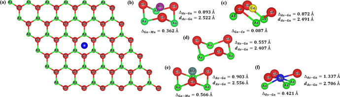
Figure 1. Oblique view of the considered systems: (a) top view of a transition-metal adatom at the hollow site of 551-GaAs supercell, and side views of the optimised placements for the absorbed (b) Mn, (c) Co, (e) Mo, and (f) Os atoms at such a site. For comparison, panel (d) shows relaxed buckling of 551-GaAs at the hollow site in absence of an adatom.
Download figure:
Standard image High-resolution imageIn order to study the magnetic interaction between neighbouring TM atoms, identical TM atoms were considered adsorbed on 2D-GaAs in close proximity to each other, as shown in figure 5.
The electron wave function was expanded in plane waves up to a cutoff energy of 500 eV in all the calculations. A Γ-centered grid of 25 × 25 × 1 k-points was used to sample the irreducible Brillouin zone in the Monkhorst–Pack special scheme [50], except for the 551-GaAs supercell where a 8 × 8 × 1 k-point grid was used. Grimme's method (DFT-D2) was implemented to treat long-range electronic correlations [51]. The PYPROCAR code was used to plot the electronic bands of both 2D-GaAs pristine unit-cell and TM on 551-GaAs supercell [52]. In addition, a 20 Å vacuum was kept as vertical spacing between the adjacent supercells to avoid interactions. The optimised parameters for 2D-GaAs monolayer, and the TM adsorbed on 551-GaAs are given in table 1. We have calculated the charge transference by Bader analysis [53]. In our study, the spin–orbit interaction for TM on 551-GaAs supercell has been taken into account. SOC is a relativistic interaction between moving electrons and a local electric field E created in their rest frame. From special relativity we know that in the electron frame a magnetic field B is created. Due to the interaction of B with the electron intrinsic magnetic moment, and the Zeeman effect, the orbital energy levels are split, which can lead to different transition levels with energy:

where ξ(r) = e2/2 contains the entire radial dependence of the SOC Hamiltonian operator [54, 55]. L and S are the electron orbital and spin angular momentum, respectively.
Table 1. Calculated lattice constant [a0 (Å)], angle between neighbouring bonds (θ), buckling parameter [ΔAs–Ga (Å)], vertical Ga–TM distance [ΔGa–TM (Å)], adsorption energy per TM atom (Eads), bandgap value (EG), magnetic moment per TM atom (μ), charge located on the adatom (Δρ), and MAE per TM atom, for 2D-GaAs monolayers and TM on 551-GaAs supercell (TM = Mn, Co, Mo and Os). The positive (negative) value of the MAE implies that the easy magnetisation axis is out-of-plane (in-plane) to the surface of the 2D structure.
| a0 (Å) | θ (°) | dAs–Ga (Å) | ΔAs–Ga (Å) | ΔAs–MT (Å) | Eads (eV) | EG (eV) | μ (μB) | Δρ (e) | MAE (meV) | |
|---|---|---|---|---|---|---|---|---|---|---|
| 2D-GaAs | 4.048 | 114.4 | 2.407 | 0.577 | — | — | 1.060 ΓK | — | — | — |
| (4.050) [5] | 114.3 | 2.410 | 0.550 | — | — | 1.080 ΓK | — | — | — | |
| (3.970) [42] | 114.7 | 2.380 | 0.550 | — | — | 1.290 ΓK | — | — | — | |
| Mn | 3.999 | 114.6 | 2.522 | 0.893 | 1.255 | 2.166 | 0.583 Γ Γ | 3.000 | 0.532 | 0.530 |
| Co | 3.997 | 111.8 | 2.491 | 0.872 | 0.959 | 3.539 | 0.672 ΓM | 1.000 | 0.043 | −0.950 |
| Mo | 4.000 | 117.6 | 2.556 | 0.903 | 1.469 | 2.799 | Halfmetal | 4.000 | 0.427 | 3.460 |
| Os | 3.991 | 100.8 | 2.706 | 1.337 | 0.916 | 4.967 | 0.156 MM | 2.000 | −0.411 | −6.930 |
The MAE of single TM on 551-GaAs was calculated using the following expression

where E∥ and E⊥ are total energies for the in-plane and out-of-plane magnetisation directions with respect to the surface of the 2D crystal, respectively [22]. Table 1 displays the calculated MAE per TM atom of our systems.
To obtain magnetic exchange interactions between two adsorbed metal atoms, we employed the four-state energy mapping methodology [56, 57]. Heisenberg spin Hamiltonian is considered in the form:

where  is a vector. Jij
is 3 × 3 matrix describing the magnetic exchange interaction between two magnetic sites. Jij
may be formally decomposed into three components: the diagonal part, i.e. the isotropic exchange; the antisymmetric component, also known as the DMI, whose vector D is made from off-diagonal elements of the antisymmetric exchange, and the off-diagonal elements of the isotropic exchange. Since off-diagonal elements of the isotropic exchange part are small, in this work, we will focus on the two first components: the isotropic exchange and DMI. The DMI components, i.e.,
is a vector. Jij
is 3 × 3 matrix describing the magnetic exchange interaction between two magnetic sites. Jij
may be formally decomposed into three components: the diagonal part, i.e. the isotropic exchange; the antisymmetric component, also known as the DMI, whose vector D is made from off-diagonal elements of the antisymmetric exchange, and the off-diagonal elements of the isotropic exchange. Since off-diagonal elements of the isotropic exchange part are small, in this work, we will focus on the two first components: the isotropic exchange and DMI. The DMI components, i.e.,  ,
,  and
and  , were calculated by the following equations:
  ,
,  , and
, and  . All nine elements of the matrix (
 ), as well as the DMI parameters, are listed in table 2. In order to obtain the ground state spin configuration of two adatom cases, the Heisenberg spin Hamiltonian, which is constructed with the obtained magnetic exchange interaction via DFT, is solved iteratively.
Table 2. Calculated exchange matrix parameters ( ) between two TM atoms of the same type adsorbed on a 2D-GaAs (TM = Mn, Co and Mo), as well as the DMI components
  ,
,  ,
,  , the total DMI parameter |D|, the ratio between |D| and the average of diagonal exchange parameters
  ,
,  and
and  , and the calculated MAE, all defined with respect to the TM pair. The positive (negative) value of the MAE implies that the easy magnetisation axis is out-of-plane (in-plane) to the surface of the 2D structures.

|

|

|

|

|

|

|

|

|

|

|

| |D| | |D|/|Jdiag| | MAE | |
|---|---|---|---|---|---|---|---|---|---|---|---|---|---|---|---|
| (meV) | (meV) | (meV) | (meV) | (meV) | (meV) | (meV) | (meV) | (meV) | (meV) | (meV) | (meV) | (meV) | (meV) | ||
| Mn | −4.54 | −4.55 | −4.56 | −0.27 | −1.56 | 1.46 | 0.55 | −0.04 | 0.04 | 0.64 | 0.46 | −0.04 | 0.79 | 0.17 | 1.03 |
| Co | −8.05 | −0.01 | −6.73 | −0.22 | −0.53 | 2.08 | −2.04 | −0.20 | 0.47 | 0.15 | 2.06 | −0.33 | 2.09 | 0.42 | −0.54 |
| Mo | 3.50 | 3.49 | 3.54 | 0.11 | −0.09 | −0.07 | 0.06 | −0.28 | 0.27 | 0.10 | −0.06 | −0.27 | 0.30 | 0.09 | 2.89 |
Literature suggests an alternative Liechtenstein, Katsnelsson, Antropov and Gubanov formalism (LKAG) approach to find the magnetic exchange parameter for ferromagnetic metals and alloys [58], however this method does not yield information about anisotropic interactions and DMI. We therefore use 4SM method, due to our interest extended beyond the isotropic magnetic exchange interactions, also to the induced DMI when TM adatoms are adsorbed on 2D-GaAs semiconductor and inversion symmetry is broken. 4SM method has been shown to be particularly effective for this purpose [59].
3. Results and discussion
3.1. Energetic stability and structural properties
We first calculated the adsorption energy of a single TM adatom (Mn, Co, Mo and Os) on a 551-GaAs supercell and examined the stability of our systems using the following expression

where E(TM–GaAs) and E(GaAs) are the total energies of the system with adsorbed TM atom and 551-GaAs supercell respectively, and E(TM) is the energy of a single isolated TM atom. More stable structures have a larger adsorption energy. We found that the preferential location of all the TM adatoms studied in our work is the hollow site (within the hexagonal Ga–As tile), followed by the site on top of As as the second most favourable. Os atom is metastable on both sites, with an energy difference of ∼284 meV. We have chosen the hollow site as the location for adsorption of the TM atoms, because it combines the best energetic and structural stability. Table 1 displays the adsorption energies on hollow site for comparison. The energy stability order of our studied configurations is as follows: Os (4.967 eV/adtom), Co (3.539 eV/adatom), Mo (2.799 eV/adatom), and Mn (2.166 eV/adatom). We note that all configurations exhibit comfortably large energetic stability.
Subsequently, we investigated the local structural distortions introduced by the adatom in the supercell. The optimised structural parameters for pristine 2D-GaAs crystal structure and TM on 551-GaAs are given in table 1. In addition, figure 1 depicts a top view for TM centered above one hollow site (middle of Ga–As hexagonal tile) of the 551-GaAs supercell (figure 1(a)), as well as the side view of the relaxed buckling for Ga and As atoms (ΔAs–Ga) located at the hollow site for 551-GaAs supercell in absence of any adatom (figure 1(d)). Furthermore, the optimised placements for Mn, Co, Mo and Os atoms (ΔGa–TM) are shown in figures 1(b), (c), (e), and (f), respectively. One sees from table 1 that the optimised structural parameters for pristine 2D-GaAs (a0) are in good agreement with previous theoretical reports [5, 42]. When one TM atom is adsorbed on the 551-GaAs supercell, the relaxed unit-cell lattice parameter of TM on 551-GaAs system (a0' = asup/5) is reduced slightly when compared with the one of pristine unit-cell, i.e. by 1.21, 1.26, 1.19, and 1.41%, for Mn, Co, Mo and Os adatom, respectively. This can be explained by the larger buckling parameter (ΔAs–Ga) for TM adsorbed on 551-GaAs when compared with the one of pristine 2D-GaAs. The nearest As–Ga bond (dAs–Ga) is larger for TM on 551-GaAs than the one in pristine 2D-GaAs by 4.78, 3.94, 6.19, and 12.42%, for Mn, Co, Mo and Os atom, respectively.
From the analysis above, one can see that Os (Z = 76) and Mo (Z = 42) atoms, which have higher atomic numbers and are larger, result in a larger buckling (ΔAs–Ga) and extend As–Ga bonding length (dAs–Ga) compared to the cases of Mn (Z = 25) and Co (Z = 27). The optimised placements for Mn, Co, Mo and Os atoms (ΔGa–TM) are shown in figuress 1(b), (c), (e), and (f), respectively. The Mn and Mo atoms remain above the hollow site at a vertical distance of, respectively, 0.362 Å and 0.566 Å from the Ga-plane, while Co is almost in Ga-plane (0.087 Å from Ga-plane) and Os is located between As-plane and Ga-plane, nearer to the Ga-plane (ΔOs–Ga = 0.421 Å and ΔAs–Os = 0.916 Å). These differences in TM distance from Ga-plane (As-plane) can be intuitively explained by the electronegativity difference between TM and Ga (As) atoms. Mo (Os) and Mn (Co) are the most (least) electropositive atoms, thus Ga–Ga (As–As) in-plane distance increases (decreases) due to charge repulsion (attraction) when a more electropositive atom is adsorbed. This expansion (contraction) of Ga–Ga (As–As) in-plane distance can be evidenced by the increase (decrease) of the angle between neighbouring bonds (θGaAsGa) for Mo (2.797%) and Mn (0.175%) (Os: −11.888% and Co: −2.797%) when compared to the one of the pristine system, as shown in table 1. As a result, Mo and Mn atoms experience a lower net electrostatic force towards the Ga-plane (As-plane) when compared to Co and Os atoms. In table 1 we also give the charge located on the TM adatom (Δρ), which is consistent with the difference of electronegativity between the constituent elements.
3.2. MAE and electronic properties
As shown in table 1, the adsorbed single adatom induces a magnetic ground state in the nonmagnetic 2D-GaAs system, with a net magnetic moment of 3.0 μB, 1.0 μB, 4.0 μB, and 2.0 μB per TM atom for the case of Mn, Co, Mo and Os adatom, respectively. Table 1 also shows the calculated MAE per TM atom of our systems. The positive (negative) value of the MAE implies that the easy magnetisation axis is out-of-plane (in-plane) to the surface of the 2D structures. One sees that Os atom induces the largest MAE (−6.930 meV), followed by Mo (3.460 meV), Co (−0.950 meV), and Mn (0.530 meV). However, as would be expected, we find that a higher magnetic moment does not necessarily lead to a higher MAE, e.g., Os with a moment of 2.00 μB has a higher MAE than Mo (4.00 μB) and Mn (3.00 μB). The physical reasons that lead to MA in 2D TM-adsorbed GaAs will be analyzed in the next paragraphs. For Os adsorbed on the metastable As-top site, we found a strikingly large MAE of −28 meV.
In order to provide fundamental insights into the interaction of a TM adatom with the 2D-GaAs host semiconductor (TM = Mn, Co, Mo and Os), and how those interactions can induce magnetocrystalline anisotropy, both the electronic band structure of pristine 2D-GaAs, and the ones of Mn, Co, Mo and Os adsorbed on the hollow site of 2D-GaAs were calculated for comparison. The parametric projected electronic band structures for both the pristine 2D-GaAs sheet and the adsorbed TM on 2D-GaAs are shown in figures 2 and 3, respectively. Notice in figure 2 that 2D-GaAs has a K–Γ indirect band gap of 1.06 eV. In the projected plots, the colour intensity corresponds to the degree of overlapping of sp orbitals between Ga and As atoms. The yellow lines, near and below the Fermi level, represent the contributions of As-4pz
orbitals. The unfilled band, near and above the Fermi level (green lines), represents the contribution of Ga-4pz
and Ga-4s orbitals. The buckling reduces the sp2 (pz
orbitals) hybridization, and increases the sp3 one (pz
and planar s). Figure 3 displays the parametric orbital projected electronic structure for TM on 2D-GaAs [TM = Mn (a), Co (b), Mo (c) and Os (d)]. Electronic structure analysis shows that the semiconducting nature of pristine 2D-GaAs is retained by Mn (Γ–Γ), Co (M–Γ) and Os (M–M) systems, with bandgap energy reduced by 45%, 37% and 85%, respectively. On the other hand, adsorption of Mo on 2D-GaAs changes its nature to a half-metallic one. One sees in figure 3 that the TM adatom creates localised states near the Fermi level. In the projected plots, the colour intensity corresponds to the degree of contribution of the d-electrons of the TM adatom. The Ga and As atoms surrounding the adatom lead to a crystal field splitting of the d orbitals of the TM adatom. Due to the buckling of 2D-GaAs, and the different electronegativities and atomic numbers between TM, Ga and As atoms, the crystal-field splitting of the d orbitals of the TM on 2D-GaAs deviates from the known planar trigonal-level splitting. In the case of crystal-field splitting of trigonal planar geometry, if the ligand atoms lie in the x–y plane, the dxy
and  orbitals have the highest energy because their electron density is concentrated in the x–y plane. The
  orbital has higher energy than the dxz
and dyz
orbitals. The physical reason of this feature is the ring of electron density that
orbital has higher energy than the dxz
and dyz
orbitals. The physical reason of this feature is the ring of electron density that  orbital has in the x–y plane. The dxz
and dyz
orbitals of the central TM adatom have the lowest energies because they have all their electron density out-of-plane.
orbital has in the x–y plane. The dxz
and dyz
orbitals of the central TM adatom have the lowest energies because they have all their electron density out-of-plane.
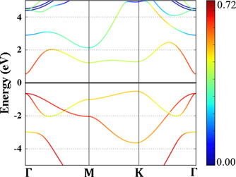
Figure 2. Parametric orbital projected band structure of pristine 2D-GaAs. The colour intensity corresponds to the degree of overlapping of sp orbitals between Ga and As atoms. Fermi energy is set to 0 eV.
Download figure:
Standard image High-resolution image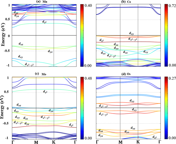
Figure 3. Parametric orbital projected band structure of TM on 2D-GaAs, calculated with SOC included. The colour intensity corresponds to the degree of contribution of the d orbital of a TM adatom. Fermi energy is set to 0 eV.
Download figure:
Standard image High-resolution imageFor the cases of Co and Os, which exhibit magnetisation in the in-plane direction, the orbitals of higher energy levels are dxy
and  , as shown in figures 3(b) and (d), respectively. Due to different vertical position of Co and Os adatom with respect to the Ga-plane and As-plane, see figures 1(c) and (f), respectively, the energies for
  and dxz
(dyz
) orbitals differ. While the
and dxz
(dyz
) orbitals differ. While the  orbital for Co has a somewhat higher energy than that of the dxz
and dyz
orbitals, for Os we find the opposite, the energies for dxz
and dyz
orbitals are higher than that of
orbital for Co has a somewhat higher energy than that of the dxz
and dyz
orbitals, for Os we find the opposite, the energies for dxz
and dyz
orbitals are higher than that of  . Another difference between these cases is the large overlap among the dxz
and dyz
orbitals of Co and 4-px
py
pz
-GaAs orbitals as compared with those for Os, as shown in figure 3(b) by green lines. This can be explained by the closer distance between Co and Ga-planes as compared to distance of Os to the Ga-plane. Regarding the electronic structure of Mn and Mo on 2D-GaAs, one notices in figures 3(a) and (c), respectively, that dxz
and dyz
are the occupied states of higher energy, followed by dxy
and
. Another difference between these cases is the large overlap among the dxz
and dyz
orbitals of Co and 4-px
py
pz
-GaAs orbitals as compared with those for Os, as shown in figure 3(b) by green lines. This can be explained by the closer distance between Co and Ga-planes as compared to distance of Os to the Ga-plane. Regarding the electronic structure of Mn and Mo on 2D-GaAs, one notices in figures 3(a) and (c), respectively, that dxz
and dyz
are the occupied states of higher energy, followed by dxy
and  . This can explain the out-of-plane magnetisation axis for both those TM adatoms on 2D-GaAs.
SOC plays a fundamental role in the magnetic behavior of the TM-adsorbed on 2D-GaAs semiconductor. The SOC mechanism works as follows: figure 2 displays s and p mixed orbitals of pristine 2D-GaAs near the Fermi level, both in the valence and in the conduction bands. Structural buckling reduces the overlapping between pz orbitals. As a result, the sp3 hybridization near Fermi level becomes stronger than sp2. On the other hand, the outermost d-orbital of TM ions are half-filled and, by Hund's rule, they are aligned parallel. When TM ion is adsorbed on 2D-GaAs semiconductor, the local magnetic moment of d-TM states hybridizes with the sp bands near the Fermi level of 2D-GaAs (spin–orbit interaction). Therefore, the sp–d exchange interaction between the sp band electrons of 2D-GaAs and the d electrons associated with the TM atoms, as well as the lack of inversion symmetry of the crystal environment, are the responsible of the magnetic behavior of TM-adsorbed on 2D-GaAs semiconductor.
The calculated electronic spin–charge density for systems with the easy magnetisation axis parallel [(a) Os and (b) Co] and perpendicular [(c) Mn and (d) Mo] to the surface of the considered 2D structures is shown in figure 4. The colour intensity represents the spin–charge density, where blue and red indicate high and low density, respectively. The magnetic moment in each of these systems mainly originates from the adatom, i.e. 63, 95, 68 and 53% of total magnetisation for Mn, Co, Mo and Os atom, respectively. Conversely, the magnetic moment stemming from the nearest neighbours at the hexagonal Ga–As tile where adatom resides is smaller than that found in adatom case, i.e. 4.9, 4.5, 10 and 37% of total magnetisation for Mn, Co, Mo and Os system, respectively. Thus, according to our results, the MA of TM on 2D-GaAs system depends robustly on the broken crystal symmetry, the orbital character of the states in the vicinity of the Fermi level, and the magnitude of the interaction of the spins with the field generated by the electron orbital motion in the crystal.
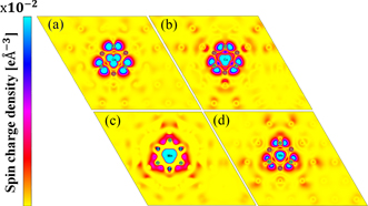
Figure 4. Calculated electronic spin–charge density for systems with the easy magnetisation axis in-plane [(a) Os and (b) Co] or out-of-plane [(c) Mn and (d) Mo] to the surface of the 2D structure. The colour intensity represents the spin–charge density, where blue and red indicate high and low electronic spin–charge density, respectively.
Download figure:
Standard image High-resolution image3.3. Magnetic exchange interaction
During experimentally performed adsorption, one expects multiple adatoms to reside in close proximity to each other. The study of small clusters is of special scientific interest due to their unique magnetic properties can be tailored for desired applications in magneto-electronics by choosing a special size or composition of the cluster. That in turn opens questions about the nature of magnetic interaction arising between the adsorbed atoms in a close range from each other.
Modern DFT-based calculations are able to describe the electronic and magnetic properties of the transition metal clusters in excellent agreement with the value obtained from the experimental ones. For instance, the experimental study of magnetic properties of Co atoms adsorbed on graphene [60] agrees very well with the ones predicted by DFT [61]. In addition, Stroppa et al reported that computational images of Mn defects on GaAs predicted by DFT are consistent with the experimental ones [62].
We therefore set out to determine the magnetic exchange interaction between two neighbouring transition-metals adatoms on 2D-GaAs, by calculating the generalised 3 × 3 matrix according to equation (3). We will primarily focus on two components of the magnetic exchange interaction: the isotropic exchange and the DMI.
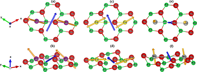
In order to examine the magnetic exchange interaction between two adsorbed transition metal atoms in close proximity to each other, we first relaxed the structures for the first (4.05 Å) and second nearest distance (7.01 Å) between TM atoms (MnMn, CoCo, and MoMo) adsorbed on 2D-GaAs. The second nearest distance was chosen as subject of this study, as shown in figure 5, instead of the nearest one, because its geometry was not distorted at the hexagon site after relaxation as for the nearest case. Then, we calculate the magnetic exchange parameters for the most stable geometry ( ) using DFT methodology described in section 2. All nine elements of the matrix (
 ), as well as the DMI parameters
  ,
,  ,
,  , the total DMI parameter |D|, and the ratio between |D| and the average of the diagonal exchange parameters
  ,
,  and
and  , are listed in table 2. Ratio |D|/|Jdiag| gives one insight in how strong D is as compared to the isotropic exchange J [yielding standard (A)FM behavior].
Figure 5. Top and side view, of interacting TM adatoms on 2D-GaAs: Mn (a) and (b), Co (c) and (d), and Mo (e) and (f) atoms, located at the hollow sites of a 551-GaAs supercell. DMI vector D12 (blue), showing non-trivial magnetic exchange interaction between the two TM adatoms is also shown, together with their spins (vectors in gold) at ground state for facilitated sense of orientation.
Download figure:
Standard image High-resolution image
Our results show that the total magnetisation obtained for Co (1 μB/adatom) is smaller than those for Mn (3 μB/adatom) and Mo (4 μB/adatom) atoms. The pairwise distances between Co, Mn and Mo adatoms after relaxation are, respectively, 6.68 Å, 6.77 Å, and 7.16 Å. One can see that for our three magnetic systems, the magnetic exchange interaction is stronger as the TM adatoms reside closer to each other. The optimised position of the two adatoms has the same physical tendency as for the single adatom cases. The Mn and Mo atoms remain above the hollow site to a vertical distance of 0.469 Å (0.362 Å) and 0.611 (0.566 Å) from Ga-plane, respectively, while Co resides in the Ga-plane (0.087 Å from Ga-plane). The values given in parenthesis represent the corresponding distances for the case of a single adatom, for comparison. When two TM atoms are adsorbed on the 551-GaAs supercell, the relaxed unit-cell lattice parameter of TM on 551-GaAs system (a0' = asup/5) is reduced slightly when compared with the one of the pristine unit-cell, i.e. by 1.48 (1.21), 1.58 (1.26) and 1.24 (1.19)%, for Mn, Co and Mo atoms, respectively (the values in parenthesis are for single adatom cases). The optimised structural parameters for a pair of adatoms therefore exhibit the same physical tendencies as the previous single-adatom cases.
As shown in table 2, the magnetic interaction between adjacent TM adatoms significantly changes the emergent magnetic properties. One sees that Co prefers the FM ground state, with the magnetisation along the x-axis, and exhibits a strong FM interaction in both x and z directions, as  = −8.05 meV and
  = −6.73 meV. Such difference of diagonal elements points to strong anisotropy. Regarding the Mn system, FM interaction is also found. The difference between all diagonal elements differs only by 0.01 meV, meaning there is almost no anisotropy. On the other hand, there is an AFM interaction found between two Mo atoms on 2D-GaAs, with a slight anisotropy favouring the z-(out-of-plane) direction. We found for all three systems that
  ,
,  , and
, and  , which indicates that the matrix J12 is antisymmetric. Furthermore, the off-diagonal elements of the exchange matrix are all different from zero, in agreement with the antisymmetry considerations by Moriya [34]. The consequent magnitudes of |D| for Mn, Co, and Mo pairs of adatoms are, respectively, ∼17%, ∼42%, and ∼9% of the average symmetric exchange interaction, as shown in table 2. Hence, DMI is both stronger and more influential in the case of Co adatoms, compared to Mn and Mo adatoms. While having a weaker magnetic moment, Co hosts larger SOC and therefore enhances the DMI interaction. Table 2 also displays the calculated MAE with respect to the TM pair of our systems. The positive (negative) value of the MAE implies that the easy magnetization axis is out-of-plane (in-plane) to the surface of the 2D structures. We can see that Mo atom induces the largest MAE (2.89 meV), followed by Mn (1.03 meV) and Co (−0.54 meV). As for the single adatom cases, the easy magnetization axis of Co and Mo (Mn) atoms in two adatom cases remains in-plane and out-of-plane, respectively. Figure 5 depicts orientation vectors for both the spins at ground state (gold colour) and DMI (blue colour) of the magnetic exchange interaction for each studied pair of TM atoms absorbed on 2D-GaAs. The ground state spin configurations are obtained by solving Heisenberg spin Hamiltonian iteratively. We note once more that D vector tends to align the neighbouring spins orthogonally to each other, instead of the parallel or antiparallel spin alignments obtained by the usual Heisenberg exchange interaction. The direction of the induced magnetisation on 2D-GaAs semiconductor can be selectively manipulated depending on chosen TM adatoms. The induced DMI in the TM-adsorbed GaAs monolayer causes spins of adjacent TM atoms to deviate from perfect (anti)ferromagnetic alignment. As a consequence, spins prefer non-collinear, chiral magnetic ordering, enabling spin textures unattainable otherwise. That is in turn attractive for development of spintronic devices, for example those based on special properties of spin-waves, with dispersion tailored by local DMI.
Finally we observe that Os adatoms in close proximity to each other the magnetisation vanishes on each Os atom, and the system goes to a non-magnetic state. Therefore, Os atoms coupling neither FM nor AFM in a close range from each other. This result strongly differs from our calculations for single Os adatom, where the system is comfortably magnetic with 2 μB magnetisation. It is therefore clear from these results that magnetic properties of adatoms strongly depend on the density of adatoms, and that more studies are needed to fully characterize the magnetic properties of specific patterns and densities of TM adatoms on 2D-GaAs. Furthermore, taking into consideration that the magnetic interactions may change drastically with distance [63], the study of the distance dependent magnetic exchange interaction of TM-adsorbed 2D-GaAs will be explored in further research.
4. Conclusions
We investigated the structural and electronic properties, as well as the magneto-crystalline anisotropy energy and magnetic exchange interactions of different transition metal adatoms (Mn, Co, Mo and Os) on 2D-GaAs using first-principles and the four-state energy mapping methodologies based on DFT. Electronic structures analysis upon structural relaxation revealed that the indirect K–Γ semiconducting nature of the pristine 2D-GaAs can be tuned by adsorption of transition metal atoms. We also found that the transition metal adatom leads to a magnetic ground state in otherwise nonmagnetic 2D-GaAs system. More specifically, even a single TM adatom gives rise to high magneto-crystalline anisotropy energy, exhibiting either in-plane (e.g. Os, 6.93 meV) or out-of-plane MAE (e.g. Mo, 3.46 meV) for TM adsorbed on the central site above a hexagonal Ga–As tile. MAE can increase dramatically for TM adatoms trapped at a metastable site, as demonstrated in case of Os on As-top site leading to a giant in-plane MAE of 28 meV. According to our results the arising MA of TM on 2D-GaAs stems from the broken crystal symmetry, the orbital character of the states in the vicinity of the Fermi level and the spin–orbit interactions in the crystal. One notices however that same arguments can be put forward to justify appearance of the DMI, crucial for appearance of non-collinear magnetic textures beyond the standard ferro-antiferro dichotomy. For that reason, we examined in detail the magnetic interactions between a pair of identical transition-metal atoms adsorbed on 2D-GaAs. For Co adatoms, we found a FM ground state with in-plane MA, as well as strong DMI. For either Mn and Mo adatoms placed on adjacent adsorption sites, almost no anisotropy is found. Still, Mn retains FM interaction, while Mo adatoms exhibit AFM interaction. On the other hand, a pair of Os adatoms, in same locations as other TM pairs, fall into a non-magnetic ground state (despite the single adatoms being strongly magnetic). This clearly indicates that both the concentration and ordering of TM adatoms play a crucial role in their induced magnetic features in 2D-GaAs. Bearing in mind the versatility of magnetic features we reported in the case of different TMs, and the need for magnetic textures by design for applications in e.g. magnonics, our findings provide a useful foundation for further theoretical and experimental tuning of 2D magnetic materials based on III–V systems (the latter already being a proven commodity in spintronic applications).
Acknowledgments
This work has been carried out with financial support of Universidad del Norte and Colciencias (Administrative Department of Science, Technology and Research of Colombia) under Convocatoria 712—Convocatoria para proyectos de investigación en Ciencias Básicas, año 2015, Cod: 121571250192, Contrato 110-216. The authors also acknowledge support from the Special Research Funds of the University of Antwerp (BOF), and the Research Foundation-Flanders (FWO). Part of the calculations were performed within the VSC (Flemish Supercomputer Center), funded by the FWO and the Flemish Government—department EWI.
Data availability statement
All data that support the findings of this study are included within the article (and any supplementary files).
Conflict of interest
There are no conflicts to declare.