

Abstract
Synchrotron x-ray diffraction measurements on powder 2H-MoTe2 (P63/mmc) up to ∼46 GPa have been performed along with first-principles based density functional theoretical analysis to probe the isostructural transition in low pressure regime and two electronic topological transitions (ETT) of Lifshitz-type in high pressure regime. The low pressure isostructural transition at ∼7 GPa is associated with the lattice parameter ratio c/a anomaly and the change in the compressibility of individual layers. The pressure dependence of the volume by linearizing the Birch–Murnaghan equation of state as a function of Eulerian strain shows a clear change of the bulk modulus at the ETT pressure of ∼20 GPa. The minimum of c/a ratio around 32 GPa is associated with the change in topology of electron pockets marked as second ETT of Lifshitz-type. We do not observe any structural transition up to the maximum applied pressure of ∼46 GPa under quasi-hydrostatic condition.
Export citation and abstract BibTeX RIS
1. Introduction
Transition metal dichalcogenide (TMD) materials have attracted renewed interest following the recent discovery of Weyl semimetallic phases of both I- and II-types with the non-trivial electronic topological signatures [1–7]. Layered TMDs with the common formula MoX2, where X is a chalcogen element (S, Se, Te), consist of X–Mo–X sheets being stacked along c-direction and held together by van der Waals (vdW) interaction. The commonly studied structural form of TMDs is the semiconducting hexagonal phase (2H) where Mo atoms are trigonal-prismatically coordinated by the chalcogenide atoms [8]. One of the unique properties of these MoX2 compounds is that they can exist in different structural forms (polymorphism) such as 2H, 1T, 1T', 3R and Td
-type lattices with different electronic properties [9, 10]. Few layer 1T'–MoTe2 having monoclinic crystal structure with a bandgap [11] of ∼60 meV is predicted to be a potential platform to study the  -topological quantum devices [12]. In case of three-dimensional (3D) topological insulators of A2B3 types (A = Bi, Sb; B = Se, Te), it is the rhombohedral phase [13–15] which holds
  -electronic topological signatures whereas for TMDs, it is the orthorhombic phase which shows non-trivial Weyl-topological signatures of type-II reflected in the observation of Fermi arcs on the surface [3, 5, 16], providing a potential route in realization of quantum spin Hall effect. Recently, superconductivity is observed in Td–MoTe2 with Tc
= 8.2 K at 11.7 GPa leading to a new pathway for the exploration of topological superconductivity [17, 18]. In addition, monolayer TMDs (direct band gap) have inequivalent valleys at the corners of the Brillouin zone which mark them as potential candidates for two-dimensional valleytronics [19, 20] as well as optoelectronics [21] at room-temperature [22, 23].
-electronic topological signatures whereas for TMDs, it is the orthorhombic phase which shows non-trivial Weyl-topological signatures of type-II reflected in the observation of Fermi arcs on the surface [3, 5, 16], providing a potential route in realization of quantum spin Hall effect. Recently, superconductivity is observed in Td–MoTe2 with Tc
= 8.2 K at 11.7 GPa leading to a new pathway for the exploration of topological superconductivity [17, 18]. In addition, monolayer TMDs (direct band gap) have inequivalent valleys at the corners of the Brillouin zone which mark them as potential candidates for two-dimensional valleytronics [19, 20] as well as optoelectronics [21] at room-temperature [22, 23].
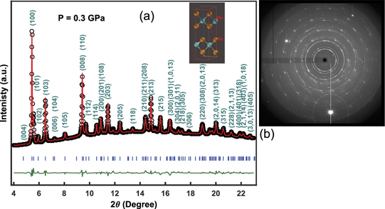
Figure 1. (a) Rietveld refinements algorithm used to match the patterns to P63/mmc crystal structure at 0.3 GPa with the GSAS II software package. The experimental data are indicated by black circles, the calculated pattern is the red solid line, and the lower curve drawn in dark-green is the weighted difference between the observed and calculated pattern. The profile factor Rp = 0.64% and the weighted profile R-factor Rwp = 0.99%. Inset shows the unit cell stacking of atoms along c-direction. (b) Corresponding two-dimensional XRD image at 0.3 GPa.
Download figure:
Standard image High-resolution image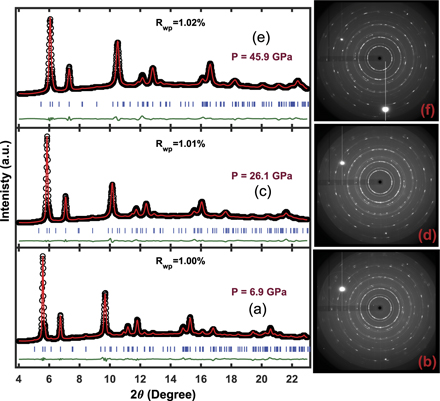
Figure 2. Rietveld refinement patterns to P63/mmc crystal structure at (a) 6.9 GPa, (c) 26.1 GPa and (e) 45.9 GPa with the GSAS II software package. The profile Rp-factors (and Rwp) are for (a) 0.71% (1.01%), (b) 0.68% (1.01%) and (c) 0.69% (1.02%). The corresponding two-dimensional XRD images at (b) 6.9 GPa, (d) 26.1 GPa and (f) 45.9 GPa are also shown.
Download figure:
Standard image High-resolution imageTuning among different polytypes and thereby changing their electronic properties is attractive from application point of view such as making ohmic contacts by using homojunction [24] between the metallic and semiconducting phases of TMDs; varying the concentration of W in solid solution of Mo1−x
Wx
Te2 to induce semiconducting-2H to metallic-Td phase at room temperature [25]; and semiconducting-2H to metallic-1T' phase via charge carrier doping [26]. Applying pressure is one of the proven routes to induce structural polytypes as observed in 2H-MoS2 (P63/mmc) for which, the onset of lateral shift of the adjacent S−Mo−S layers is around ∼20 GPa leading to a mixed phase of 2Hc
(2H) and 2Ha
structures with the 2Hc
-phase being the dominant one [27] and thereby changes the pressure coefficients of the Raman modes [28]. The layer sliding transition in MoS2 from 2Hc
(semiconductor) to 2Ha
(metal) completes at ∼40 GPa [28]. Recently, it has been shown that the Mo-based ternary chalcogenide MoSSe (P63
mc) also undergoes isostructural layer sliding transition from 2Hc
' to a mixed phase of 2Hc
' + 2Ha
' around 11 GPa [29]. However, it was shown [30] experimentally as well as theoretically that the similar compound MoTe2 (P63/mmc) does not undergo structural transition up to the maximum reached pressure of 30 GPa. Even high pressure Raman and x-ray diffraction (XRD) studies on MoSe2 (P63/mmc) [31] confirm that there is no structural transition up to 36 GPa. Recent Raman spectroscopic measurements as well as density functional theoretical (DFT) calculations showed [30] that the bulk 2H-MoTe2 undergoes two transitions as a function of pressure: at ∼6 GPa and 16.3 GPa associated with semiconducting to semimetallic transition and electronic topological transition of Lifshitz-type, respectively. It is worth noting that electronic topological transitions (ETT) of Lifshitz-type is quite distinct in topological sense from the ETT of  -type, involving dynamical corrections to the anomalous signatures of phonon modes [14].
For 2H-MoTe2, we showed [30] that reliable Raman data from diamond anvil cell (DAC) could not be captured using the methanol–ethanol (4:1) mixture as the pressure transmitting medium (PTM), and it was attributed to the adsorption of alcohols on the surface of MoTe2 and the dissociation through thermodynamically favorable channels [32]. In this work, we report XRD studies on bulk 2H-MoTe2 as a function of pressure using Ne gas as a PTM to probe the changes in the lattice parameters around two phase transitions mentioned above where Raman modes showed changes in pressure coefficients [30]. The isostructural semiconducting to semimetallic transition coincides with a sharp decrease in the ratio c/a and the decrease of compressibility of individual layers around ∼7 GPa. The ETT of Lifshitz type at ∼20 GPa is shown to be accompanied by changes in bulk modulus. In addition to this, our study brings out another ETT of Lifshitz type around ∼32 GPa associated with a minimum in c/a ratio and linkage of electron pockets at K and K2 points (i.e. change in topology of electron pockets) in Brillouin zone.
2. Experimental and computational details
The sample of 2H-MoTe2 [30, 33] was a gently pelletized powder obtained from crushing a single crystal and pressed between two glass slides. The lateral size of the sample was ∼50–60 μm, estimated from the microscope image, with a thickness less than 60 μm (the measured thickness of the indented gasket). It was loaded along with a ruby chip inside a hole of diameter ∼150 μm in a rhenium gasket inserted between the diamonds (of culet size 300 μm) of a symmetric DAC. We confirmed that the sample thickness was well within the height of the indented gasket and it was almost in the center of the hole. High pressure XRD experiments on MoTe2 (P63/mmc, #194) up to ∼46 GPa were carried out using synchrotron radiation on beam line P02.2 [34] at PETRA-III (DESY), Hamburg, Germany. Ne gas was used as a PTM. The x-ray wavelength used for the experiment is 0.288 Å. The sample to detector distance was calibrated using LaB6. The pressure was determined using well known ruby fluorescence shift (the pressure uncertainty in our experiment is ∼±0.1 GPa). Only one small ruby (⩽10–12 μm) was loaded in the sample chamber for pressure calibration. DIOPTAS software [35] was used to integrate the Deby–Scherrer diffraction rings and to convert it into 1D pattern (intensity versus diffraction angle (2θ)). The lattice parameters (a and c) are derived from Rietveld refinements for all the XRD patterns using GSAS II software package [36]. At the end of every Rietveld refinements (after refining atomic coordinates), spherical harmonics (of order 8 to 10 with texture index ∼1.8) were used to model the preferred orientation corrections. Our first-principles calculations are based on density functional theory (for details, see reference [30]).
3. Results and discussion
Rietveld analysis of XRD pattern at 0.3 GPa is performed using GSAS II software package and plotted in figure 1(a) along with (hkl)-reflections. The Mo and Te atoms occupy 2b Wyckoff site and 4f Wyckoff site, respectively, same as for 2H-MoS2 or MoSe2 structure (P63/mmc) (see the inset of figure 1(a)). Figure 1(b) represents corresponding two-dimensional XRD image at 0.3 GPa without masking for better visualization. Figure 2 shows three XRD patterns taken at ∼6.9 GPa, 26.1 GPa and 45.9 GPa. Upon compression of MoTe2 up to ∼46 GPa, all the XRD peaks shift to larger 2θ-values (smaller d-spacings, see figures S1 and S2 in supplementary materials (https://stacks.iop.org/JPCM/33/065402/mmedia) [37]), as expected due to shrinkage of the 2H-MoTe2 lattice. We do not observe any new peak(s) in the pressure range up to 46 GPa (see figure S1(a)).
The extracted lattice parameters (a, c) are plotted as a function of pressure in figures 3(a) and (b). The c-axis shows faster decrement up to ∼7 GPa and then it slows down. The compression of c-axis is stronger than the a-axis as expected for an anisotropic layered material where stacked layers along c are connected via weak vdW interactions. By fitting 3rd order Birch–Murnagham (BM) equation of state [38, 39] (see equation (1)), the obtained compressibility's at ambient pressure (and pressure derivative of bulk modulus) for c-axis and a-axis are ∼4.7(1) × 10−3 GPa−1 ( = 25.9 ± 2.8) and ∼1.6(01) × 10−3 GPa−1 (
 = 13.2 ± 0.3), respectively. The c-axis and a-axis are reduced by ∼14.2% and 10.3 %, respectively over the whole pressure range of 46 GPa in agreement with the report by Zhao et al [40]. Figure 3(c) shows the variation of ratio c-to-a as a function of pressure displaying following changes: (i) sharp decrement of c/a by ∼0.12 within the first 7 GPa (marked by an arrow); (ii) from 7 GPa, it goes to a minimum value around ∼32 GPa followed by an increment in c/a (by ∼0.03) up to the maximum applied pressure of 46 GPa. The sharp decrease in c/a at ∼7 GPa in accordance with the reported [30] semiconducting to semimetallic transition is related to the decrease in interlayer spacing and hence induced semi-metallicity because of Te-orbitals overlap.
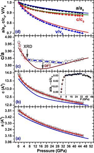
Figure 3. Here, points and solid lines are used for XRD and DFT calculated data, respectively. The pressure variations of lattice parameters a, c and c/a ratio are shown in (a), (b) and (c), respectively. The red solid lines in (a) and (b) represent fitting of 3rd order BM equation of state. Pressure dependent normalized lattice constants and the unitcell volume are plotted in (d). Error bars, less than the size of the data points, are also plotted. The inset of (b) shows the plot of (a/a0–c/c0) as a function of pressure.
Download figure:
Standard image High-resolution imageThe normalized lattice constants along with the normalized unit cell volume are plotted in figure 3(d), and it is clear that there is no volume discontinuity up to 46 GPa. It is worth noticing from figure 3(d) that the separation between the normalized lattice constants decrease with the increase of pressure and the separation (a/a0–c/c0) is plotted in the inset of figure 3(b). Sharp increase in a/a0–c/c0 up to 7 GPa, to a maximum in a/a0–c/c0 around 32 GPa and then decrement up to 46 GPa corroborates with the c/a data.
Now, we present our DFT calculated lattice parameters (a, c) variations with pressure (solid blue lines in figures 3(a) and (b)). It is clear that compression of c-axis is faster than that for a-axis for first 8 GPa. From figure 3(c), we mark (shown by an arrow) another transition around 18 GPa where calculated c/a ratio goes to a minimum (discussed later in detail). The calculated normalized lattice parameters (see figure 3(d)) show that the separation between a/a0 and c/c0 decreases with the increase of pressure in corroboration with our experimental observations.
The ratio of interlayer (Te–Te) to intralayer (Mo–Te) distance is plotted in figure 4(a); showing clearly that up to 7 GPa, the ratio decreases rapidly implying that the interlayer vdW distance reduces leading to quasi 3D solid-network beyond 7 GPa. We mark another transition around 20 GPa where the ratio changes its slope. Here, it is worth to monitor the Te atom positions with pressure as only z-coordinate of Te position (z–Te) is allowed to vary (Mo atom is fixed) according to the constraints imposed on Wyckoff positions by space group P63/mmc. The individual layer compressibility (ILC) [41] is related to z–Te atom and the rate of ILC (−1/z(dz/dP)Te) is plotted in the inset of figure 4(a) clearly showing a rapid decrease up to 7 GPa and after that it varies very slowly in linear fashion up to ∼20 GPa. This in-turn also indicates that the Te–Te orbitals start to overlap and beyond 7 GPa the Coulomb repulsion prevails to slow down the rate. Our marking of 7 GPa from XRD data for semiconductor to semimetal transition coincides with the recent high pressure transport measurements where it has been shown that the resistivity ratio (ρ300K/ρ2K) goes above 1 around 9 GPa [40] which is 2 GPa higher, probably due to the non-hydrostatic component of PTM (Daphne oil 7373) [40]. Our DFT calculated ratio of interlayer (Te–Te) to intralayer (Mo–Te) distance is plotted in figure 4(b) which brings the above mentioned two transitions at ∼8 and 18 GPa, respectively. The calculated ILC (see inset of figure 4(b)) also marks the two transitions in agreement with our experimental observations. Both experimentally observed and calculated ILC show qualitatively similar trends along with its almost invariant behavior after ∼32 GPa. The robustness of our XRD-refined z–Te is further confirmed by comparing with the DFT calculated values as a function of pressure (see figure S3 for details).
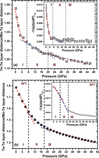
Figure 4. The ratio of interlayer (Te–Te) to intralayer (Mo–Te) distance is plotted as a function of pressure for (a) XRD refined and (b) DFT calculated values. Here, Rietveld refined coordinates are used to calculate the distances. Error bars, less than the size of the data points, are also plotted. Insets of (a) and (b): rate of ILC are plotted. The red dashed curves in (a) correspond to the fitting using f(P) = p + qP + rP2, where p, q and r are constants. Three different regions are marked as I, II and III.
Download figure:
Standard image High-resolution imageThe P–V data (figure 5(a)) is fitted with the third-order BM equation of state [38, 39]:
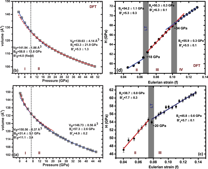
Figure 5. (a) XRD refined and (b) DFT calculated P−V data are shown. The fitted lines using 3rd-order BM equation are shown in solid lines. Error bars, less than the size of the data points, are also plotted in (a). (c) XRD refined and (d) DFT calculated reduced pressure H vs Eulerian strain (f) plots. The transition regions at which H changes its slope are marked in gray rectangular areas; the crystal structure remains the same up to maximum observed pressure of ∼46 GPa. Marked LT represents Lifshitz transition. Here, regime I is excluded where trivial semiconductor−semimetallic transition occurred. Four different regions are marked as I, II, III and IV.
Download figure:
Standard image High-resolution imageFrom the fitting up to 7 GPa (semiconductor−semimetal transition), the bulk modulus at ambient pressure B0 is 31.4 ± 5.1 GPa, its pressure derivative B0' = 11.1 ± 3.4 and the ambient pressure volume V0 = 150.56 ± 0.37 Å3. From the fitting from 7 GPa to maximum pressure, those values are B0 = 57.3 ± 2.6 GPa, B0' = 4.9 ± 0.2 and V0 = 146.73 ± 0.56 Å3. The bulk modulus is higher in the metallic phase as compared to the semiconducting phase [40]. For DFT calculated P−V values and the corresponding fitted values (B0, B0' and V0) are shown in figure 5(b). Around 8 GPa (semiconductor to semimetal transition), we could not get appreciable B0 values from our DFT calculated PV-values: before 8 GPa, B0 = 58.8 ± 11.8 GPa and V0 = 141.94 ± 1.86 Å3 (using 2nd order BM equation) and after 8 GPa, B0 = 63.3 ± 21.9 GPa, B0' = 5.3 ± 1.3 and V0 = 139.63 ± 4.14 Å3 (using 3rd-order BM equation).
The ratio of interlayer (Te−Te) to intralayer (Mo−Te) distance and ILC both show a transition around 20 GPa. The transition at ∼20 GPa coincides with the LT seen in our recent DFT studies [30] on 2H−MoTe2 where ETT has been marked by the abrupt appearance of electron and hole pockets. Near ETT, no volume discontinuity (first derivative of Gibbs free energy) is expected but the changes in second derivatives of Gibbs free energy such as compressibility is expected to occur. Therefore, a better way to capture the signatures of subtle structural changes is to express equation (1) in terms of Eulerian strain (f) and reduced pressure (H) [38]:

where, f =  , X =
, X =  and reduced pressure H = P/{3f(1 + 2f)5/2}.
The reduced pressure H scales linearly with Eulerian strain f. In absence of a transition, H is linearly dependent on f. Figure 5(c) shows the slope change of H at ∼20 GPa (marked as LT) where the changes of B0 and B0' are also marked in figure 5(c): B0 = 38.7 ± 0.8 GPa and B0' = 7.7 ± 0.3 before the LT, B0 = 45.8 ± 0.6 GPa and B0' = 5.7 ± 0.1 after the LT. Therefore, the discontinuity observed in H–f plot indicates that there are subtle structural modifications attributed to the electronic structure evolution seen in DFT calculations on 2H-MoTe2 [30]. Our calculated reduced pressure vs Eulerian strain also confirms the ETT of Lifshitz-type around 18 GPa with another clear transition at ∼34 GPa as shown in figure 5(d). As we know that there are no structural transitions or volume discontinuity for MoTe2 [30] around 32 GPa (see figures 3(d) or 5(a)), therefore the possibility could be related to the changes in the electronic structure.
From our electronic structure calculations, we find that hole pocket appears at M-point at P ∼ 30 GPa in addition to hole pockets seen at Γ and a points observed at 20 GPa [30] (figures 6 and 7). Further increase in pressure leads to an increase in the size of the hole pocket at M point. The bands forming electron pockets at K and K2 points intersect (or cross) each other in the vicinity of K2 point as shown in figure 6(a). At 30 GPa, this crossing of the band is just above the Fermi level which moves toward the Fermi level with increasing hydrostatic pressure. At 34 GPa, it is at Fermi level which leads to interesting change in Fermi surface topology. To probe this further, we investigate the evolution of the Fermi surface with pressure. At 34 GPa, the hole pockets are observed at M-point (see figure 7(a), the blue pockets at the center of the sides of the hexagon) and the electron pockets are seen at K and K2 points (figure 7, the purple pockets mark the electron pocket). We find the Fermi surface associated with the bands at K and K2 points changes (topology of the Fermi surface) at an applied hydrostatic pressure of P ∼ 34 GPa (see figures 7(b)–(d)). Since, the Fermi surface changes with applied pressure without breaking the structural symmetry, we assign it to a LT at P ∼ 34 GPa. Therefore, our observed minimum in c/a ratio at 32 GPa (see figure 3(c)) is associated with the second LT. The electronic band structures at a few low pressures ( ∼6, 12, 18 and 24 GPa) are shown in figure S4 [37].
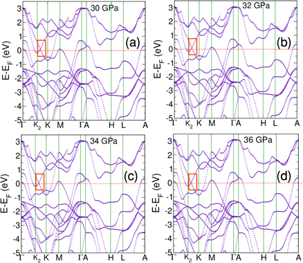
Figure 6. Electronic structure of 2H-MoTe2 at (a) 30 GPa, (b) 32 GPa, (c) 34 GPa and (d) 36 GPa. The highlighted areas show the band crossing moves toward Fermi level with increasing hydrostatic pressure.
Download figure:
Standard image High-resolution image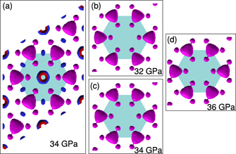
Figure 7. Fermi surfaces at (a) 34 GPa of merged bands (all the bands crossing the Fermi levels). Panels (b), (c) and (d) show the electron pocket of Fermi surface changing with pressure at P = 32 GPa, 34 GPa and 36 GPa respectively. Note that (b), (c) and (d) show the electron pockets at K and K2 points with pressure. Note that purple color pockets show electron pockets whereas blue and red pockets (at the center and center of the sides of the hexagon) show hole pockets.
Download figure:
Standard image High-resolution image
4. Conclusions
In summary, high pressure XRD measurements have been performed along with first-principles based DFT analysis to show low pressure isostructural and high pressure two electronic topological transitions of Lifshitz-type. Semiconducting to semimetallic transition at ∼7 GPa is related to the sharp decrease in c/a ratio and in rate of compressibility of individual layers. DFT-predicted electronic topological transition of Lifshitz-type at ∼20 GPa is accompanied by the changes of bulk modulus as deduced in the reduced pressure vs Eulerian strain plot. The minimum in c/a ratio at 32 GPa is associated with the second LT. We hope that our work will stimulate further high pressure transport studies as well as thermoelectric measurements to capture the anomalies near the LT at ∼20 and 32 GPa.
Acknowledgments
High pressure x-ray experiments were carried out at PETRA III beamline, Germany (DESY) and we gratefully acknowledge DESY, a member of the Helmholtz Association HGF, for providing experimental facilities. AKS acknowledges the funding from Department of Science and Technology (DST) and JC Bose National Fellowship, India. We thank the Department of Science and Technology (DST), India for financial support to carry out the experiments at DESY, Germany. UVW thanks DST support through a JC Bose National Fellowship and Sheikh Saqr Fellowship. AB is thankful to IISc for a postdoctoral fellowship.