
Abstract
In order to meet the requirement of spintronic and optoelectronic, we have systematically investigated the effect of Mn doping and co-doping of Mn with C on the electronic, magnetic and optical properties of wurtzite zinc sulfide (ZnS) using first principle calculations. Our results find that single Mn doping alters the non-magnetic ZnS to a magnetic one and keeps its semiconducting and a semiconductor to half-metal transition is observed for Mn–C co-doping. Furthermore, an antiferromagnetic (AFM) and ferromagnetic (FM) ground states are favorable for Mn-doped and Mn–C co-doped system, respectively. Additionally, the optical properties of our studied configuration have been calculated in terms of real and imaginary parts of the complex dielectric function, absorption coefficient, and reflectivity. The absorption edge shifts slightly toward lower energy and intensity of the main peak become weak for single Mn doping, and a sharp peak at low energy is observed for the Mn–C co-doping. The analysis of optical absorption of Mn ions doped system shows the blue- and red-shifts of the d-d transition in the AFM and FM coupled of Mn ions doped configuration, respectively which is in good agreement with the experimental observations. The improved magnetic and optical properties of Mn–C co-doped ZnS shed light on the future application of such kind of materials in spintronic and optoelectronic devices such as remote sensing and photovoltaics.
Export citation and abstract BibTeX RIS
1. Introduction
The group II–VI semiconductors have been investigated intensively because of their potential applications in optoelectronics. These materials served in establishing marketable electronic and optoelectronic devices working in the entire spectral regions. They show their potential visual displays, high-density optical memories, transparent conductors, solid-state laser devices, photodetectors, solar cells, etc [1–3].
Dilute magnetic semiconductors (DMSs) have received much attraction in the field of condensed matter physics and material sciences due to the potential application in the spintronic devices. These materials utilize both properties charge and spin of electrons to perform their multifunction. DMSs, which are fabricated by doping non-magnetic semiconductors with magnetic impurities such as transition metals (TMs) or rare earth metals up to few percents, are considered to be ideal candidates for the spintronic devices [4–6]. These materials based devices have been used in many fields for examples, spin-based transistors, mass storage devices, hard disk drive heads, spin valves, magnetoresistance sensors used in computers [7]. For the practical applications, DMSs must have ferromagnetism at room temperature. The possibility of room temperature ferromagnetism in Mn-doped ZnO and GaN predicted by Deitl et al [8] motivated other researchers to investigate the behaviors of ferromagnetic materials above the room temperature. During past years, the most studied DMSs with room temperature ferromagnetism is Mn-doped GaN [9], Mn-doped ZnO [10], and transition metals (TMs) doped TiO2 [11]. The ferromagnetism in DMS arises from spin-carrier exchange interaction between the host charge carriers and magnetic ions [12, 13]. For the spin-polarized transport application, the metallic DMS structure is needed, but for the luminescence application, the semiconducting DMS structures are favored, though few studies on the latter type have been reported. In common knowledge, the spin-related optical emissions are usually found in wide-band DMS structures [6, 14].
Among the other II–VI semiconductors, ZnS has attracted attraction due to its wide band gap and its potential applications in electronic and optoelectronics such as blue light emitting diodes, optical coating, solar cells, and especially photovoltaic devices. The zinc sulfide (ZnS) exists into two structures: wurtzite structure with band gap 3.77 eV and other is zinc blende structure or cubic structure with band gap 3.72 eV [15–17]. ZnS shows large exciton binding energy 38 meV compared with room temperature thermal energy 30 meV; therefore, it is an extraordinary material for room temperature exciton devices [18]. In experiments, the results show that Mn+2 doped ZnS semiconductors are luminescent materials, which have a wide range of application in electroluminescence, displays, and spin light-emitting diodes [19, 20]. Therefore, Mn+2 doped ZnS reveals several interesting magneto-optical and magnetic properties. Many experiments have confirmed that ZnS is a promising host material for achieving room temperature ferromagnetism. For examples, Cu doped ZnS [21] and Co-doped ZnS [22] are reported to be room temperature ferromagnetic materials. Recently, the magnetic properties of TMs doped cubic ZnS were investigated theoretically and found that Ni, Cr, and V in DMSs interact ferromagnetically while Co and Mn couple antiferromagnetically but the coupling between Fe ions shows competition between FM and AFM [23]. Most recently, Kamran et al [24] investigated experimentally the correlation of magnetic and luminescence properties of Mn-doped ZnS nanobelts. There exists some discrepancy in the ferromagnetic properties of Mn-doped ZnS. For examples, the paramagnetism in Mn-doped ZnS was reported by Ming et al [25]. Tsuijji et al [26] observed the absence of antiferromagnetism at low temperature. However, EPR studies by Lakshmi et al [27] shows the ferromagnetic behavior around room temperature. However, such a discrepancy in the ferromagnetic properties shows that the appearance of ferromagnetism in Mn-doped DMSs are still unclear [28, 29]. In order to understand the existing controversy of ferromagnetism in Mn-doped ZnS, we should investigate the properties of Mn-doped ZnS with C co-doping.
Furthermore, there are several theoretical works on the magnetic properties of nonmetals doped ZnS [21, 30]. It is found experimentally and theoretically that the co-doping of non-metals (N, and C) and Mn in semiconductors is an effective method to induce ferromagnetism above the room temperature [31–34]. This motivates us to investigate the effect of hole doping introduced by C co-doping in Mn-doped ZnS to achieve high-temperature ferromagnetism for spintronic applications.
In this theoretical work, we have studied the electronic magnetic and optical properties of C and Mn co-doped ZnS using the first-principles calculations. It has been found that Mn-doped ZnS is a magnetic semiconductor while Mn–C co-doped ZnS is half metal ferromagnetic. We also explained the magnetic coupling between Mn ions in Mn-doped ZnS and C and Mn co-doped ZnS.
2. Theoretical model and method of calculations
The calculations reported here were performed by using periodic, spin-polarized density functional theory (DFT) using projector-augmented wave (PAW) potentials [35, 36], implemented in VASP package [35]. We used the Generalized Gradient Approximations (GGA) with Perdew–Burke–Ernzerhof (PBE) functional to treat the exchange-correlation potential [37]. But GGA approximation gives underestimated band gap and do not give the correct position of d or f states of TMs or rare earth metals. In order to improve the bandgap of ZnS and to describe the correct position of d-state of a transition metal, we used the GGA + U method. The Hubbard U describes the on-site interaction of coulomb potential. The interaction of coulomb potential may be attractive or repulsive, depending on the sign of U. The positive U is used to describe the on-site repulsive coulomb potential and the negative U for on-site attractive coulomb potential. Moreover, the positive U is suitable for the localized state such as d-state of Zn and increases the repulsive coulomb potential, while negative U is suitable for the delocalized state such as p-state of anion and increases the attractive coulomb potential [38–40]. First, we investigate the effect of U parameter for d-state of Zn on the band structure (BS) of ZnS. For this, we calculate a set of DOS for different U parameters for d-states as shown in figure 1(a). The bandgap energy values increase from 2.1 to 2.53 eV when U value on Zn-3d state is changed from 0 to 7.5 eV. It also depicts that Ud lowers the energy of Zn-3d states with respect to the Fermi level and reduces the hybridization effect where it is overestimated by GGA functional, and consequently, the bandgap energy increases. When Ud > 8 eV, the bandgap energy can be improved further, but the position of Zn-3d become more localized than the experimental value. Thus, the problem of the incorrect position of Zn-3d can be resolved with appropriate Ud, but the problem of bandgap energy underestimation is still unresolved.
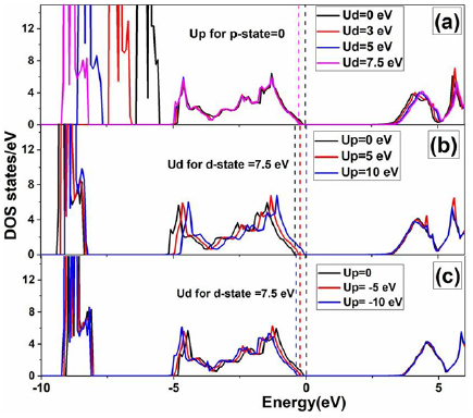
Figure 1. Density of states of ZnS as a function of effective on-site parameters Ud and Up for Zn-3d and S-3p states, respectively. The vertical dashed lines indicate the Fermi levels.
Download figure:
Standard image High-resolution imageA bandgap energy can be improved significantly, if in addition to the Ud value for Zn-3d states the Up value is incorporated for S-3p states as well in our GGA + U calculations. Note that the effect of Up value on the position of Zn-3d state is very small. First, we confirm that appropriate Up for p -state is either positive or negative. To confirm this, we calculate DOSs for positive and negative Up for p -state of S atom. Figure 1(b) shows the set of DOSs corresponding to different positive Up parameters for S-3p states in addition to Ud = 7.5 eV. We can see that the Fermi level shifts upward with positive Up parameters. It means that positive Up shifts the valence band maxima (consists of p -orbitals) upward and decreases the bandgap energy. Thus, Up > 0 is not suitable for improving the bandgap energy. In figure 1(c), we can see that negative Up shifts valence band maxima downward and increases the bandgap energy. Thus, the negative values of Up are appropriate to improve the bandgap energy in GGA + Ud + Up method. This method is called GGA + USIC; SIC stands for self-interaction correction [40]. After several calculations for a different negative value of Up with Ud = 7.5 eV, we found the pair of Ud = 7.5 and Up = −15 eV was identified as an appropriate value for the band structure (BS) of ZnS semiconductor. The negative Up values were also employed for p -state of anion in CdTe and ZnSe [40, 41].
The description of the d-state of the transition metal can be improved significantly in the magnetic semiconductor by Hubbard-U corrections to GGA or LDA [42]. We have performed several calculations using 2 × 2 × 2 ZnS supercell containing single Mn dopant to optimize the Hubbard term U for Mn-3d states. By comparing with experimental results of optical d-d transitions, we found that U = 1.2 eV for Mn-3d states was known as the best choice for optical results of Mn-doped ZnS. Here, in this work, we use U = 1.2 eV for Mn-3d states to study magnetic and optical properties. The energy cutoff, energy change and maximum force on each atom were set at 600 eV, 0.000 01 eV and 0.01 eVÅ−1 respectively in all the calculations. For unit cell 1 × 1 × 1, a Gamma-centered k-point mesh of 10 × 10 × 6 and 14 × 14 × 10 was used for sampling the Brillouin Zone (BZ) for structure relaxation and electronic and optical calculations. For 2 × 2 × 2 supercell, a Gamma-centered k-point mesh of 5 × 5 × 3 and 7 × 7 × 5 was employed for structural relaxation and electronic and optical calculations.
3. Result and discussion
3.1. Electronic structure of pure ZnS
In order to compare our calculated results with other reported results, first, we investigate the properties of pure ZnS. The calculated lattice constants are a = 3.82(3.76) Å and c = 6.23(6.17) Å with GGA(GGA + U) methods. The lattice constants calculated with GGA are in close agreement with experimental values (a = 3.82Å and c = 6.26Å) [43] and theoretical reports [44]. We found that the GGA + U method produces smaller lattice constants than the GGA method, which is due to the fact that the application of Hubbard term U produces the d-states more localized. The calculated average bond length Zn–S is 2.33(2.31) Å with GGA(GGA + U) methods. The calculated bond length with GGA is in line with a theoretical report [44]. The following calculations were performed with the GGA + U method.
To understand the electronic structure of wurtzite ZnS, we calculate the BS along high symmetry direction of the first BZ and electronic density of state (DOS) using GGA + U method. From figure 2(a), one can see that ZnS is a semiconductor with a band gap of 3.32 eV. Also, the valence band maximum (VBM) and conduction band minimum (CBM) occurs at Г symmetry point indicating the direct band gap nature of pure ZnS, which can be used in optical devices [3].
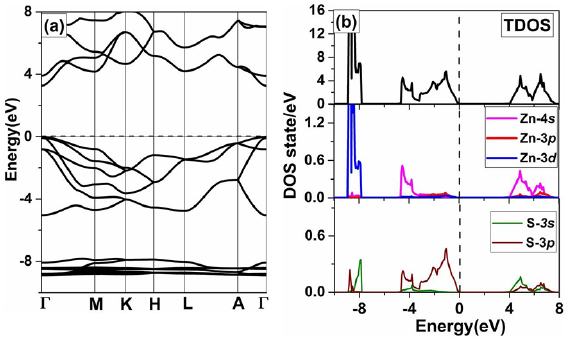
Figure 2. (a) the calculated BS and (b) density of state (TDOS/PDOS) of pure ZnS. The Fermi level is represented by a horizontal/vertical dashed line and is set at zero energy.
Download figure:
Standard image High-resolution imageTo further insight the electronic properties of pure ZnS, we have calculated the total and projected density of states, as shown in figure 2(b). From the total density of state (TDOS), we can see that the valence band is divided into two parts. The width of the upper and lower parts of the valence band are 4.2 eV and 1.3 eV respectively. From the PDOS of ZnS, one can see that the valence band maxima (VBM) are mainly contributed by the 3p states of S near the Fermi-level. But the lower part of the valence band is mainly contributed by Zn-3d states. The main peak of Zn-3d state at −8.89 eV matches with experimental report (−8.97 eV) [45]. On the other hand, the major contribution to the bottom of the conduction band comes from Zn-4s states, and small contribution is observed from s-states of the S atom. Additionally, we performed the spin-polarized calculation of pure ZnS and found no spin polarization.
3.2. ZnS with doping
3.2.1. Stability with single Mn doping.
To induce a magnetic ground state in pure ZnS, we doped Mn atom at Zn-site as shown in figure 3(a). It is found experimentally that TMs like Co, In, and Pt can be doped in solid material by pulsed laser deposition [46]. If one Zn atom is replaced by Mn atom in the host supercell of 2 × 2 × 2, leading to 6.25% Mn concentration. After relaxation, the calculated the average bond length Mn–S is 2.38Å, which is smaller than that of Zn–S because of the difference in the atomic size of Mn and Zn.
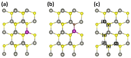
Figure 3. The relaxed structures ZnS doped with (a) single Mn (b) (Mn, C) co-doped ZnS and (c) ZnS supercell with labels x, y , and z indicate the sites for C doping and labels 1, 2 and 3 indicate the site for Mn doping for the description of different configurations in Mn–C co-doped system. The gray, yellow, purple and brown balls represent the Zn, S, Mn, and C atoms respectively.
Download figure:
Standard image High-resolution imageIn order to check the stability of the Mn-doped ZnS, first we performed magnetic and non-magnetic ground state calculations, and we find that the magnetic ground state is more favorable than the non-magnetic ground state of the doped system. The formation energy for Mn-doped ZnS can be calculated by the following relation

Where  , and
, and  are the total energies of Mn-doped ZnS and pure ZnS respectively. The chemical potential
  of Mn dopant is equal to the total energy per Mn atom in bulk structure while chemical potential
  depend on the growth conditions, Zn-rich and S-rich conditions. In order to estimate the chemical potential
  , we use the relation
  . For Zn-rich condition,
  is equal to the total energy of Zn per atom in the hexagonal crystal structure and for S-rich condition,
  is equal to
  where
where  (total energy of S per atom in the S8 structure) and
  (total energy of pure ZnS per formula unit). Therefore, the formation energy of Mn-doped ZnS is +1.74 eV under Zn-rich condition while that is −6.65 eV under S-rich condition. The negative formation energy means that under S-rich condition Mn-doped ZnS is easier to fabricate than that in Zn-rich condition.
3.3. Electronic and magnetic properties ZnS with doping
3.3.1. ZnS with Mn doping.
To see the effects of Mn doping on the electronic and magnetic properties, we have calculated spin-polarized BS and density of state (DOS). In figure 5(a), we have shown spin-polarized BS, which is calculated along high symmetry direction (Г-M-K-H-L-A-Г) of the first BZ. The calculated band gaps are 2.82 eV and 3.34 eV for up-spin and down-spin channels, respectively.
In order to understand the electronic properties of Mn-doped ZnS system in more detail, we computed the total density of state (TDOS) of Mn-doped ZnS and partial density of states (PDOS) of 3d-states of Mn atom and 3p-states of the nearest-neighboring S atoms as a function of energy as shown in figure 5(b). The calculated TDOS shows asymmetric distribution between up-spin and down-spin channels, which demonstrates the spin polarization for Mn-doped ZnS system. According to crystal field theory 'the 3d-state of Mn is decomposed into two sub-states' one is doubly degenerate states  (
( ,
,  ) and other is triply degenerate state
  (
( ,
,  ,
,  ) under the action of the tetrahedral field formed by S-atoms around Mn ion'. But for the hexagonal structure, the d-state is divided into three states e1 (
 ,
,  ), e2 (
 ,
,  ) and a (
 ). Since Mn dopant has five electrons in 3d-state. According to Hund's rule, these sub-states are filled with the five up-spin electrons, so these states located below the Fermi energy level are shown in the PDOS of Mn-3d state. These five up-spin electrons in 3d-states are responsible to induce the spin polarization in the system with the total magnetic moment of 5 µB. The spin-down channel of these sub-states are empty, and therefore located the above the Fermi energy level. Near the Fermi level, the 3d-states of Mn play an important role in the magnetic properties. We see that near the Fermi-level, Mn-3d states hybridize with S-3p states. Due to this p -d hybridization, the up-spin and down-spin channels at the valence band are unbalanced and the spin-polarization induces in the system. In figure 4(b), we plot 3D iso-surface of spin density for a single Mn doped ZnS system. It can be seen clearly that the spin density distribution is largely localized on Mn dopant and distributed over the nearest neighboring S atoms which indicates that the wave function of the Mn-3d states is spatially extended to the nearest neighboring S atom and interact to the 3p states of S atoms. We can also see that Mn doping polarizes the neighboring S atoms in the same direction. It can be seen that a large portion of magnetization is localized around Mn and little localized around non-magnetic sites Zn and S due to p-d hybridization. Due to this p-d hybridization, the local magnetic moment of Mn is reduced to 4.30 µB. Xie [44] obtained similar results for a local and total magnetic moment in his first principle study of magnetic properties of the Mn doped wurtzite-ZnS. The magnetic moment on each atom in Mn doped ZnS supercell is tabulated in table 1. The small magnetizations induced at non-magnetic sites Zn and S (nearest neighboring S and Zn atoms of Mn) are due to the sharing of electronic charge through hybridization between Mn-3d states and the bands of the host semiconductor [47].
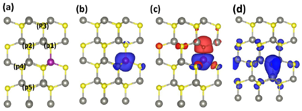
Figure 4. Supercell of Mn-doped ZnS with labels P1, P2, P3, P4, and P5 indicate five different positions for C-doping (a) The 3D iso -surface of the Spin density of 0.018 e/Å for single Mn-doped ZnS (b), Mn–C co-doped ZnS (c) and C-doped ZnS (d).
Download figure:
Standard image High-resolution image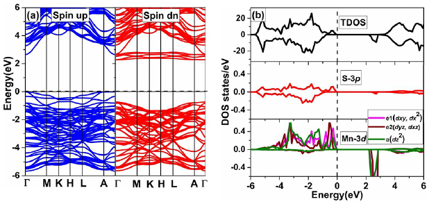
Figure 5. The spin-polarized (a) BS and (b) TDOS of Mn-doped ZnS and PDOS of Mn-3d and nearest neighboring 3p-states of S atoms. The Fermi level is represented by a horizontal/vertical dashed line and set at zero energy.
Download figure:
Standard image High-resolution imageTable 1. The total magnetic moment of supercell  (
( ) and local magnetic moments
  (
( ) on each atoms Mn and its nearest Zn, and S atoms and, C in Mn-doped and Mn–C co-doped and pure ZnS configurations.
| Systems |  |
 |
 |
 |
 |
|---|---|---|---|---|---|
| Pure ZnS | 0.00 | 0.00 | — | — | 0.00 |
| Mn-doped ZnS | 0.012 | 0.02 | 4.30 | 5.00 | |
| Mn–C co-doped ZnS | −0.026 | −0.024 | 3.64 | −0.43 | 3.00 |
| C doped ZnS | 0.066 | 0.046 | — | 0.85 | 2.00 |
In order to study the interaction between Mn ion and bands of the host semiconductor, we calculated the exchange constants Noβ and Noα. The Noβ shows the interaction of valence band of the host with magnetic ion (p-d-coupling) and Noα indicates the interaction of conduction band with magnetic ion (s-d coupling). These two parameters are very important for the analysis of band edge splitting and p-d hybridization. The band edge splitting depends upon the value of exchange constants and depends on the concentration of magnetic impurities (n). On the basis of mean field theory, these two exchanges constants can be determined by using the following relations
and
N0β and N0β are exchanged constants and  and
and  are the valence band edge and conduction band edges splitting respectively and
  is one half of the total magnetization. The calculated
  and
and  are −0.48eV and 0.12eV respectively. Using these value in the above two equations (2) and (3), the obtained value of
  and
and  are −4.16 eV and 0.51 eV respectively. The negative value of N0β indicates that coupling between magnetic moment on dopant atom and band electrons is attractive and thus antiferromagnetic. And the positive N0α shows that s-d interaction is repulsive and ferromagnetic [48].
To investigate magnetic interaction between the spins of Mn ions in Mn-doped ZnS system, two Mn atoms are substituted at the Zn sites in Mn-doped ZnS supercell, leading 12.5% concentrations of Mn in the system. As sketch in figure 3(c), two configurations 'near' and 'far' with substitutional sites (1,2) and (1,3) respectively are considered. The separation between two Mn ions is 3.76 Å in near configuration and 6.16 Å in the far configuration. For each configuration, we calculated the energy difference between AFM (ant-parallel spin orders) and FM (parallel spin orders) states. This energy difference is used to indicate the stabilization of the magnetic ground state. If the FM state energy is lower than AFM state energy, then the stable magnetic ground state is FM state otherwise AFM state. The calculated energy difference (ΔE) between AFM and FM states in near and far configurations are −187.5 meV and −6 meV respectively. We see that in both configurations, the energy difference (ΔE) is negative i.e. the AFM energy is smaller than the energy of FM state, which indicates that AFM state in both configurations is stable. Our finding is consistent with the experimental report [29]. From the total energy calculations for AFM states in both near and far configurations, we found that near configuration is lower in energy than far configuration, it demonstrates that near configuration is most stable.
We have performed one calculation for 3 × 3 × 2 ZnS supercell doped with two Mn atoms separated by one S atom in order to confirm that our results are consistent and to be close to the concentration of dopants used experimentally. Doping two Mn atoms at Zn sites in the supercell leads to 5.6% Mn concentrations, which are close to the ones used in the experiments [29, 49]. We calculate the energy difference between AFM and FM states and found that ΔE is −92 meV. It means that the total energy for the AFM state is 92 meV lower than the FM state, showing that the ground state is AFM. Therefore, our analysis remains valid for a wide range of Mn concentration in the system.
Figure 6 depicts the density of states DOSs for 12.5% Mn-doped ZnS in stable configuration (near) with AFM state. One can see that the system shows semiconducting behavior in the AFM state. It is portrayed that unoccupied d-states of Mn atoms are at 2.32 eV above the Fermi level. It means that Mn-doped ZnS system in AFM configuration absorbs 2.32 eV during the optical d-d transition, which is in good agreement with the experimental study of Mn-doped ZnS nanobelts [24]. It is interesting to note that the Mn doping at Zn sites does not produce holes around the Fermi level to mediate long-range FM coupling. Therefore, the interaction between Mn spins is AFM under the super-exchange mechanism [50]. In super-exchange interactions, no electronic hopping is taking place between Mn ions during interactions.
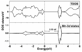
Figure 6. The partial density of state PDOS of Mn-doped ZnS in the configuration I with AFM state.
Download figure:
Standard image High-resolution image3.3.2. ZnS with (C, Mn) co-doping.
Before determining electronic and magnetic properties of (Mn C) co-doped ZnS, we first calculate the total energy for (Mn C) co-doped system with C atom at five different positions as shown in figure 4(a). In table 2, the calculated results are listed. We can see that the total energy of (C, Mn) co-doped with C atom position at P1 is lower than that for other positions. This depicts that the C atom prefers to locate near the Mn atom. We also see that the energy difference at P2, P3, P4, and P5 are close to one another. This means that the interaction between C atom and Mn atom in (C, Mn) co-doped ZnS system is insensitive to the distance once the distance exceeds 2.35 Å.
Table 2. The energy difference ΔE (eV) between C at position P1 and C at other positions P2, P3, P4 and P5 in Mn–C co-doped ZnS. These positions of C in (Mn, C) co-doped ZnS are shown in figure 4(a).
| Systems | P1 | P2 | P3 | P4 | P5 |
|---|---|---|---|---|---|
| Mn–C codoped | 0 | 1.3211 | 1.3223 | 1.3219 | 1.3209 |
When C atom is substituted at S site at the P1 position, then we optimize the structure of C, Mn co-doped ZnS. The optimized structure is shown in figure 3(b). After optimization, the bond length between C–Zn and C–Mn are 2.09 Å and 1.92 Å respectively.
For structure stability of C, Mn co-doped ZnS, we calculate the formation energy using the following equation

Where  , and
, and  are the total energy of (C, Mn) co-doped ZnS,and pure ZnS respectively.
  ,
,  ,
,  and
and  are the chemical potentials of Zn, S, Mn, and C respectively. The calculated formation energies for (Mn C) co-doped ZnS in Zn-rich and S-rich conditions are 7.25 eV and −1.17 eV respectively. The formation energy under S-rich condition is negative, which indicates that C, Mn co-doped ZnS can be easily fabricated experimentally under S-rich condition. Thus, the ferromagnetism in Mn doped ZnS can be induced by co-doping with C atom in S-rich condition.
For the investigation of the electronic structure for (Mn, C) co-doped ZnS with C atom at position P1, we calculated the energy BS along high symmetry direction as shown in figure 7(a). We can see that (Mn–C) co-doped ZnS is half-metallic material since the up-spin channel crosses the Fermi level and therefore, the material can be used in a spintronic device for producing spin-polarized current [51]. In co-doped ZnS system, the band edges splitting ΔEv and ΔEc are +0.16 eV and +0.11 eV respectively. Therefore, the calculated N0α and N0β are +0.70 eV and1.02 eV, respectively.
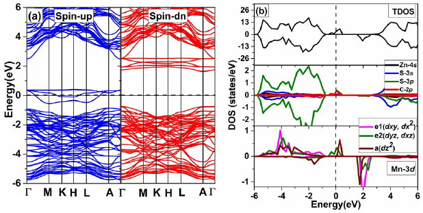
Figure 7. The spin-polarized (a) BS and (b) total and projected density of state of Mn–C co-doped ZnS. The Fermi level is represented by a horizontal/vertical dashed line and set at zero energy.
Download figure:
Standard image High-resolution imageIn order to shed light on the electronic structure of (C, Mn) co-doped ZnS in detail, the total density of state (TDOS) and partial density of state (PDOS) for (Mn, C) co-doped system are calculated and shown in figure 7(b). Compared to ZnS doped with Mn, ZnS co-doped with (C, Mn) is half metallic. The defects level appears at the Fermi-level, mostly contributed by the 3p -states of S and C and 3d-states of Mn ion.
In an ionic picture, when the C atom is doped at the site of S atom, it provides two holes to the system because the C-2p state carries two less electrons than S-3p state. Thus C-atom behaves as acceptor. The Fermi level, as a result, moves downward and up-spin Mn-3d orbitals are now partially filled rather than fully filled orbitals for ZnS doped with Mn. The C-2p state in Mn–C co-doped ZnS are also partially occupied and strongly hybridized with Mn-3d (e2) orbitals. The total magnetization per supercell containing one Mn atom and one C atom is 3.00  . In order to calculate magnetization on each atom, we calculate the spherical integration of the spin density using VASP default atomic radii of Zn (1.27 Å), S (1.164Å), C (0.863Å), and Mn (1.323Å). The local magnetic moment of Mn, C, S and Zn atoms are listed in the table 1. We can see that the magnetic moment of S and C are negative and that of Mn is positive. It means that the interactions of S and C with Mn are antiferromagnetic. In figure 4(c), the spin distribution for (Mn, C) co-doped ZnS is displayed. It is clearly seen that the spin density is largely localized at the Mn and C atoms and little localized at nearest neighboring S and Zn atoms. Hence, the magnetism comes from the C and Mn atoms in Mn–C co-doped system.
Additionally, we investigate the properties of C doped ZnS. One S atom in the 2 × 2 × 2 supercell is replaced by C atom, leading to 6.25% concentration. After the structure relaxation, the local structure around the C-atom is suppressed slightly with Zn-atoms drawn closer to the C-dopant, the average bond length between C–Zn (2.08 Å) is smaller than that of S–Zn (2.31 Å). Then we calculate the total energy for spin-polarized and non-spin polarized states. We find that the total energy of spin-polarized state is 86 meV lower than the non-spin polarized state, indicating that spin-polarized state is favorable in C doped ZnS with total magnetization (2 µB) which is in good agreement with the previous report [52].
In order to show the extended spin-polarized defect states produced by C in 2 × 2 × 2 supercell of ZnS, we calculate the spatial spin distribution, as shown in figure 4(d). We can see that a large portion of the total magnetization come from the C atom. It can be seen that along with C, it is neighboring S, Zn, and next to neighboring S are also polarized with same spin direction and the spin moment is largely extended. Therefore, it can be expected that extended spin density destribution caused by C doping may play an important role to mediate the long range FM coupling between magnetic impurities in the magnetic semiconductor. Table 1 tabulates the results for the local magnetic moment of C and its nearest Zn and S atoms, which are in line with the calculated the spatial spin distribution, as shown in figure 4(d).
In order to study the magnetic coupling between Mn ions in Mn–C co-doped ZnS. We considered five different configurations C-1(1, 2, x), C-2 (1, 2, y ), C-3 (1, 2, z), D-1 (1, 3, y ) and D-2 (1, 3, z) as shown in figure 3(c). In C Configurations the distance between two Mn atoms is 3.824 Å while in D configurations, the two Mn atoms are separated by 5.25 Å. We calculated the energy difference between FM and AFM state for all configurations. The calculated energy difference between AFM and FM state for each configuration and magnetic moments of both Mn ions in (C, Mn) co-doped ZnS are listed in table 3. We found that the energy difference between AFM and FM states is positive, showing that FM states are stable in all configurations, except C-2 configuration. The total energy of C-1 is lower than that of all configurations. It means that stable ground state configuration is C-1.
Table 3. The calculated the energy difference ΔE (meV) between AFM and FM states, favorable magnetic state (MS) and local magnetic moment  (
( ) of two Mn atoms replace the Zn atoms in Mn–C co-doped supercell with the mentioned configurations. C-1, C-2, C-3, D-1,and D-2 indicate different configurations in (C, Mn) co-doped ZnS, as shown in figure 3(c).
| Configurations | ΔE | MS |  |
|---|---|---|---|
| C-1 (1, 2, x) | 720 | FM | 4.03/4.03 |
| C-2 (1, 2, y ) | −36.00 | AFM | 3.67/4.39 |
| C-3 (1, 2, z) | 98.00 | FM | 4.36/4.36 |
| D-1 (1, 3, y ) | 20.00 | FM | 3.66/4.36 |
| D-2 (1, 3, z) | 10.00 | FM | 3.71/4.40 |
In order to study ferromagnetism in C-1 for (Mn, C) co-doped ZnS, we plot TDOS and PDOS of S-3p , C-2p , Mn1-3d, and Mn2-3d, as shown in figure 8(a). After C co-doping in between two Mn atoms in configuration C-1, the material reveals a half-metallic nature with the spin up channel being metallic and the spin down channel being semiconducting. The 100% spin polarization at the Fermi level suggests that (C, Mn) co-doped ZnS may play an important role in spin injection where spin polarized current is highly desired [53]. It is found that 3d states of both Mn atoms exists at the Fermi level due to the symmetric position of Mn1 and Mn2 relative to the position of C-atom as shown in PDOS of Mn1 and Mn2 ions. We can also see that besides Mn1-3d and Mn2-3d states, C-2p, and S-3p states are also spin polarized with partial occupied states. Therefore, Zener double exchange mechanism [54] is responsible for ferromagnetic interaction between Mn spins in (Mn, C) co-doped ZnS. During the ferromagnetic coupling, the hoping of an electron from one Mn1-3d states to another Mn2-3d states is possible, provided the neighboring Mn atoms have parallel spins. Thus, the kinetic energy of the system in the FM state is lowered.

Figure 8. The total and projected density of states with configurations (a) C-1 and (b) D-1 in Mn–C co-doped ZnS with 12.5% Mn and 6.25%C concentrations.
Download figure:
Standard image High-resolution imageIt is also found that the magnetic moment of Mn in free space (5.00  ) is greater than that of Mn ions (4.03/4.03
  ) in the co-doped system. The decrease in the magnetic moment of Mn ions in the co-doped system is because of the strong interaction between Mn-3d and C-2p orbitals. From the table, we can see that both Mn ions in C-1 configuration have nearly the same magnetic moments. This is due to the fact that the C atom is located between two Mn atoms at the same distance. So the interaction of C atom with both Mn atoms are equal. The C atom, on another hand, contributes about −0.42
  magnetic moments to the system. Consequently, in C-1, the ferromagnetic state with total the magnetic moment of 8.00
  is favorable than the AFM state by 710 meV. This energy difference 710 meV is greater than that of C Mn co-doped ZnO (656.7 meV) [22].
Next, we study the long-range ferromagnetic interaction between Mn spins; we study the configuration D-1 where –C–Zn–S– along (0 0 0 1) direction separates two Mn atoms, and C-atom is bounded to one of Mn atoms. From the table 3, it can be seen that in configuration D-1, the energy difference between AFM and FM state is 20 meV. Therefore, we predict that C co-doping can induce long-range ferromagnetism in (C, Mn) co-doped system.
To discuss the cause of long-range magnetism in (C, Mn) co-doped ZnS, we plot total density of states (TDOS) of (C, Mn) co-doped ZnS and partial density of states (PDOS) of Mn1-3d and Mn3-3d states, C-2p state, and S-3p state in D-1 configuration as shown in figure 8(b). We see that the Fermi level exists around the Fermi level, showing that the system with FM state in configuration D-1 also shows half-metallic semiconducting. The Mn1-3d state in the up-spin channel is partially filled while 3d-state of Mn3 are completely filled because, with respect to the position of C-atom, both Mn1 and Mn3 have asymmetric coordination. As depicted in figure 8(b), Mn1-3d, C-2p , and S-3p states are spin polarized states with partial occupied states. Therefore, the interaction of those partially filled up-spin orbitals makes them ferromagnetic coupling, forming the configuration D-1 ferromagnetic. Due to asymmetry coordination of both Mn atoms with respect to C atom, the magnetic moment of Mn1 atom (which is bonded to C-atom) is smaller than that of another Mn3 atom (which is not bonded to C atom). Thus, the interaction of Mn1 with C atom is stronger than that of Mn3 with C-atom. This fact can be seen from PDOS that Mn1 has partial 3d-state due to strong interaction with C atom and during the interaction, electrons from 3d-state of Mn1 transfer to 2p state of C atom, so 3d-state of Mn1 atom become partial occupied and cross the Fermi energy level. We can see also that Mn3 has half-filled 3d-state. It means that no electron transfers from 3d-state of Mn3 to the 2p state of C-atom, indicating negligible interaction of Mn3 with C-atom.
In order to investigate the magnetic coupling in (C, Mn) co-doped ZnS with 5.6% Mn and 2.8% C concentrations, we have performed the additional calculation for the total energy of AFM and FM state in 3 × 3 × 2 ZnS supercell with two Mn atoms at Zn sites and one C atom at S site. We found that ground state of (C, Mn) co-doped ZnS is still FM and its energy is 738 meV lower than that of AFM state. Thus, for a wide range of concentration of Mn impurity, (Mn, C) co-doped ZnS should be ferromagnetic.
3.4. Optical properties
A number of phenomena take place when radiation passes through a medium. These phenomena are described by different parameters that measure the optical properties of the medium [55, 56]. One of the most important and basic optical parameters is a dielectric function, which is the linear response of the material to the electromagnetic radiation. The dielectric function of a material is defined as  . Where ε1(ω) and ε2(ω) are the real and imaginary part of the dielectric function. The real part of a dielectric function describes dispersion and polarized electromagnetic radiation, whereas the imaginary part describes the absorption of the radiation when it falls on the medium. The imaginary ε2(ω) and real ε1(ω) part of dielectric function can be calculated by using Kramers–Kronig relations. Other parameters such as reflectivity and optical absorption coefficient can be calculated from the real and imaginary part of dielectric functions by using the following equations
And
First, we study the imaginary part and the real part of the dielectric function for pure, Mn-doped, and co-doped configurations. The calculated results for the imaginary part of dielectric function are elucidated in figure 9(a). The peaks in the imaginary parts of the dielectric function (ε2) are produced due to the electronic transition between occupied and unoccupied states. For pure ZnS, three main peaks can be seen in the imaginary part of the dielectric function. The peak around 3.32 eV is produced due to the electronic transition from S-3p state (valence band maxima) to Zn-4s state or S-4s (conduction band minima). The peaks at 6.02 eV and 7.0 eV may be due to the electronic transition between Zn-3d and S-3p states in the valence band. After Mn doping, the main peak of the imaginary part of the dielectric slightly shifted toward lower energy but its intensity become weak. When C atom is co-doped with Mn in ZnS, two holes are created which make the 3d-states partially occupied and as a result, (C, Mn) co-doped ZnS become half metallic. Due to half-metallicity, new peaks in the low energy 0.50–1.64 eV appeared in the imaginary part of the dielectric which is similar to the peak observed in V doped GaN [57]. Thus, the transition of an electron between C-2p state and Mn-3d state within the band gap in (C, Mn) co-doped ZnS cause the peaks at 0.50–1.64 eV. The appearance of a sharp peak at low energy in the imaginary part of the dielectric reveals strong absorption, which makes it applicable for energy harvesting devices.
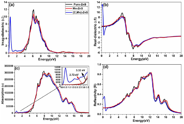
Figure 9. The calculated (a) imaginary dielectric, (b) real dielectric (c) absorption and (d) reflectivity for pure, Mn-doped and Mn, C co-doped ZnS.
Download figure:
Standard image High-resolution imageNext, we studied the real part of the dielectric function, and the results are shown in figure 9(b). We can see that the real part of the dielectric function of pure ZnS and Mn-doped ZnS are increasing constantly below 5.0 eV. But due to half-metallicity of (C, Mn) co-doped ZnS, the profile of the real part of the dielectric function is different in low energy. We can also see that the profile of ε1(ω) of pure ZnS, Mn-doped ZnS and (C, Mn) co-doped ZnS systems are similarly above 5 eV. It means that the effect of Mn doping and (Mn, C) co-doping can be shown in lower energy (<5eV). We can see that after 5 eV, ε1 starts decreasing to a negative value at 6.93 eV, 7.14 eV, and 7.06 eV for pure ZnS, Mn-doped ZnS and (C, Mn) co-doped ZnS respectively. In the negative region of the real part of the dielectric function, the materials show metallic natures and could be promising for shielding purposes.
The value of the real part dielectric function at zero energy is called static dielectric, denoted by ε1(0). The energy band gap and static dielectric are related by equation ε1(0) = 1 + (ħω/Eg)2, formulated in the form of Penn's Model [58]. According to this model, smaller the band gap of the material, higher will be its static dielectric. The static dielectric for (Mn, C) co-doped system is higher than pure ZnS and Mn-doped system. Because the spin down band gap of (Mn, C) co-doped ZnS (2.31 eV) is smaller than that of pure ZnS and Mn-doped ZnS system.
Another important optical parameter is the absorption coefficient. The absorption process is the reverse process of emission. In absorption, the electromagnetic radiation when passing through a medium is absorbed, and electrons are excited to higher states. In the emission process, the absorbed electromagnetic radiation is emitted when the excited electron becomes de-excited. For the light to be absorbed, the energy of the light must be greater than the value of the energy band gap. The absorption coefficient is calculated from the imaginary dielectric using the equation (5). Figure 9(c) presents the optical absorption coefficients of pure ZnS, Mn-doped and (C, Mn) co-doped ZnS. We can see that the optical absorption region is quite wide, and the main part of optical absorption still exists in the ultraviolet region (UV). It can be seen that several peaks above the absorption edge of pure ZnS, which are due to excitonic effects. The absorption edge of pure ZnS is at 3.32 eV which is equal to the band gap of the pure ZnS according to the BS of ZnS. Comparing with pure ZnS, the absorption edge of Mn-doped ZnS shift slightly toward lower energy. The absorption edge of Mn-doped ZnS is 2.19 eV which is due to the d-d transition. Our calculated d-d transition is in good agreement with experimental value (2.13 eV) [24]. In the d-d transition in single Mn-doped ZnS system, the electron flips from a spin up state to spin down states (figure 4). The peak at 2.73 eV (shown in the inset of figure 9(c)) in absorption spectra of Mn-doped system is due to the electronic transition between 3d-state of Mn at the top of VB and Zn-4s at the bottom of CB. Comparing with the peaks of pure ZnS, the peaks are less pronounced for Mn-doped system and (C, Mn) co-doped system. We can see a new peak (as shown in the inset of figure 9(c)) in the infrared region in (C, Mn) co-doped system which is attributed to the transition between the Mn-3d and C-2p state near the Fermi energy level or half-metallicity. We can also see that no such a peak at low energy is observed in Mn-doped ZnS because it is an insulator.
The calculated reflectivity is shown in figure 9(d). In reflectivity for pure ZnS, we see different sharp peaks in the energy range from 6.00 eV to 12.20 eV. These peaks are generated due to the excitonic effects. In doped and co-doped systems, these peaks are less pronounced and shifted slightly toward lower energy. Moreover, the reflectivity is significantly superior in the region from 6.00 to 12.2 eV energy and arise from interband transitions.
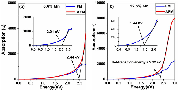
Additionally, we investigate the optical absorption during d-d transitions for FM and AFM coupled Mn-doped ZnS systems. The results for absorption coefficients are shown in figure 10. The d-d transition energy for Mn–Mn pairs in FM and AFM coupling is obtained from the electronic structure for FM and AFM configurations. In FM configuration, 3d-states of Mn is fully occupied in the up-spin channel, and 3d-states are empty in the spin-down channel. The spin of one electron flipped and the transition is from up-spin to down-spin state. The calculated optical d-d transition energy is 2.01 eV (shown in the inset of figure 10(a)) for 5.25% Mn concentration and 1.44 eV (as shown in the inset of figure 10(b)) for 12.5% Mn concentration in FM configuration, as proved by the experimental result of ZnS:Mn nanobelts (NB) [24], which is smaller than that of single Mn ion doped system (2.19 eV). Moreover, In AFM coupling, the filled up-spin state of one Mn couple with the empty up-spin state of another Mn ion. Therefore, the d-d transition for 5.25% Mn concentration is 2.44 eV, and for 12.5% Mn is 2.32 eV in AFM configuration, which also supports the experimental result [24]. Thus, the d-d transition for FM coupled Mn doping is always smaller than that for AFM coupled Mn ions doping, which could show up simultaneously in Mn-doped ZnS NB [24] and ZnSe NB [59] for their luminescence spectra.
Figure 10. The absorption spectra of FM and AFM coupled Mn ions doped systems with 5.6% (a) and 12.5% (b) concentration of Mn dopants.
Download figure:
Standard image High-resolution image
4. Conclusions
In summary, we have investigated electronic, magnetic, and optical properties of pure ZnS, Mn-doped, and Mn–C co-doped ZnS using first-principles calculations. To induce a magnetic ground state in non-magnetic ZnS, we doped it with Mn and co-doped with Mn and C. We find spin-polarization in Mn-doped and half-metallic nature is observed for Mn–C co-doping. Interestingly, the Mn-doped ZnS is a magnetic semiconductor, and Mn–C co-doped ZnS is a half-metal ferromagnetic. In coupled Mn-doped configuration, an antiferromagnetic state is favorable while the ferromagnetic state is favorable for coupled Mn–C co-doped ZnS. The absorption edge shifts slightly toward lower energy after Mn doping in pure ZnS, and the intensity of the main peak become weak. The blue- and red-shifts of d-d transition are observed in AFM coupled, and FM coupled Mn ions doped ZnS systems. The co-doping largely affects optical properties of ZnS such as absorption and reflectivity at low energy, which indicates that (C, Mn)-doped ZnS is a promising material and has potential applications in spintronics and photonic applications.
Acknowledgment
This work was supported by the 973 Project of China (No. 2014CB920903).
Conflicts of interest
There are no conflicts to declare.