
Abstract
Discussion of band gap behavior based on first principles calculations of electronic band structures for various short period nitride superlattices is presented. Binary superlattices, as InN/GaN and GaN/AlN as well as superlattices containing alloys, as InGaN/GaN, GaN/AlGaN, and GaN/InAlN are considered. Taking into account different crystallographic directions of growth (polar, semipolar and nonpolar) and different strain conditions (free-standing and pseudomorphic) all the factors influencing the band gap engineering are analyzed. Dependence on internal strain and lattice geometry is considered, but the main attention is devoted to the influence of the internal electric field and the hybridization of well and barrier wave functions. The contributions of these two important factors to band gap behavior are illustrated and estimated quantitatively. It appears that there are two interesting ranges of layer thicknesses; in one (few atomic monolayers in barriers and wells) the influence of the wave function hybridization is dominant, whereas in the other (layers thicker than roughly five to six monolayers) dependence of electric field on the band gaps is more important. The band gap behavior in superlattices is compared with the band gap dependence on composition in the corresponding ternary and quaternary alloys. It is shown that for superlattices it is possible to exceed by far the range of band gap values, which can be realized in ternary alloys. The calculated values of the band gaps are compared with the photoluminescence emission energies, when the corresponding data are available. Finally, similarities and differences between nitride and oxide polar superlattices are pointed out by comparison of wurtzite GaN/AlN and ZnO/MgO.
Export citation and abstract BibTeX RIS

Original content from this work may be used under the terms of the Creative Commons Attribution 3.0 licence. Any further distribution of this work must maintain attribution to the author(s) and the title of the work, journal citation and DOI.
1. Introduction
During recent years properties of In(Ga)N/GaN and also other nitride short period superlattices (SLs), such as GaN/Al(Ga)N and InAlN/GaN, have been intensively studied. Tens of papers have been published covering various aspects from epitaxial growth and band gap, Eg, magnitude to light emitting and laser diodes with these SLs as the active region [1–10]. In particular, a large part of the works was devoted to understanding mechanisms of radiative recombination in SLs. According to theoretical considerations, the short period (few atomic layers) SL structures make it possible to cover the significant range of visible and UV spectrum by manipulating with the quantum well (QW) and quantum barrier (QB) layer thicknesses. However, it turns out that experimental realization of these structures is very difficult.
Until recently, applied and fundamental research has been focused on InGaN, AlGaN, and much less known AlInN alloy. The main interest was concentrated on covering the spectral range of emitted/absorbed light from infrared to deep ultraviolet. The most challenging part includes preparation of InGaN with tunable energy gap in the range from Eg equal 0.65 eV (InN) to approximately 2.3 eV (In0.3Ga0.7N) crucial for optoelectronic applications from infrared to green spectral range. It is well known that ternary InxGa1−xN alloys exhibit an effect of phase separation introducing macroscopic potential nonuniformities in InxGa1−xN with x > 0.25. The pioneering work by Yoshikawa et al [2, 3] initiated the interest in binary InN/GaN SLs, appearing as an idea to solve the above mentioned difficulties. The approach consisting in the use of mInN/nGaN SLs, where m and n represent number of atomic monolayers (MLs) of InN and GaN, respectively, is very attractive since they can potentially replace InxGa1−xN alloys with high x. Because of limited amount of experimental data on InN/GaN due to difficulties in the epitaxial growth of these SLs [11, 12] many papers concentrate on theoretical considerations of their electronic band structure and structural properties [6, 7, 10, 11].
Band gap engineering, crucial for the design of optoelectronic devices, can be realized in alloys by changing the chemical composition, whereas in SLs 'tailoring' of the SL band gaps can be made by varying the layer thicknesses (m and n) and also by manipulation with lattice geometry, which we can call geometrical lattice engineering. In figure 1 we present schematically possible growth orientations of the quantum structures in the wurtzite structure. Crystal growth can be made along polar c-axis, two nonpolar directions, a and m, and six semipolar orientations (s1 to s6). We illustrate schematically the valence- and conduction-band profiles for each case. Strong internal electric fields originating from the macroscopic polarization are present in polar structure changing the shape of the band profiles and leading to small, indirect gaps in a real space. The internal electric fields are weaker in semipolar structures, and there is no built-in electric fields in nonpolar SLs. Another factor influencing the band gap behavior is the internal strain caused by lattice mismatch between QW and QB layers. Analysing the influence of all these factors on Eg values one has to keep in mind a specific feature of short period SLs, which is the effect of the QW and QB wave functions hybridization. Strong effect of hybridization is observed for thin QW and QB layers (usually up to 5–7 MLs.)

Figure 1. Schematic illustration of the geometrical lattice engineering. Polar (a), nonpolar (b) and two examples of semipolar (c) SLs are shown with the corresponding valence and conduction band profiles showing the effect of internal electric fields.
Download figure:
Standard image High-resolution imageTo realize band gap engineering it is important to understand the role of all the factors influencing the band gap behaviour and to understand their role in the evolution of Eg. In this work, based on first principles calculations, we discuss all these factors. By comparing band gaps in SLs grown along different directions of the wurtzite structure, or with different atomic arrangements, we demonstrate the effects of lattice geometry. To answer the question how the internal strain influences the Eg values, two cases of growth conditions are compared: the pseudomorphic (a-lattice constant of QW matches to QB) and free-standing (a-lattice constant of the SL is an average of QW and QB lattice constants). It will be shown in this review that assuming given growth orientation and strain conditions, the band gaps are influenced mainly by the built-in electric field, Eel (in polar structures) and by the wave function hybridization. The picture presented is somewhat simplified, but we believe that it can describe rather well the main trends in the SL band gap behavior, qualitatively and quantitatively.
In the next sections, after the description of the method of calculations in section 2, we discuss the above issues in detail. As an introduction to SL band structure calculations, and in order to obtain a suitable reference point, a short presentation of the results obtained for nitride alloys: InxGa1−xN, InxAl1−xN, and GaxAl1−xN is given in section 3. We demonstrate how to go from ordered alloy, also named in the literature as 'digital alloy', to short period SL. Then, in section 4, polar InN/GaN and GaN/AlN SLs are considered. Most of the issues discussed here are related to the polar structures grown along the c-axis (i.e.  direction) of the hexagonal wurtzite structure. We analyse the Eg evolution in free-standing and pseudomorphically grown SLs. The contributions from the internal strain, built-in electric field and wave function hybridization are evaluated. Different methods (model and ab initio) of the electric field strength evaluation are presented. It is demonstrated that the effect of wave function hybridization is dominant for narrow wells and barriers, whereas for wider layers in polar SLs the influence of the internal electric field is more important. In particular, in order to consider the oscillator strength, crucial for light emitters, we calculate the wave function overlaps. Semipolar (we choose to study in this work two directions, s2 and s6) and nonpolar SLs are considered in section 5. The results for mInN/nGaN SLs are compared with the polar case. The SLs containing alloys, as mInyGa1−yN/nGaN, mGaN/nGayAl1−yN, and mInyAl1−yN/nGaN are analysed in section 6. The band gap behavior in these SLs is compared with the gap evolution in binary SLs. As it was already pointed out obtaining mInN/nGaN SLs is very difficult [11]. Instead of intentionally introduced InN QWs likely InxGa1−xN layers are grown in such structures [12].
Using both growth method metalorganic vapour phase epitaxy and molecular beam epitaxy (MBE), QW InxGa1−xN structures with x < 0.4 are produced [13, 14]. The obtained photoemission energies for mInxGa1−xN/nGaN SLs with given In content, x, and layer widths, m and n are compared with the calculated band gaps for these SLs. As the last issue, in section 7 we compare the polar wurtzite GaN/AlN and ZnO/MgO short period SLs pointing out similarities and differences in the band gaps behavior of these two systems. In many respects GaN and AlN are similar to ZnO and MgO, respectively, especially regarding the band gaps and the lattice parameters. We found similar evolution of the GaN/AlN and ZnO/MgO band gaps with varying number of atomic MLs, whereas band gap bowings and strength of the internal electric field existing in these two families of SLs differ significantly. Finally, we conclude with a brief outlook for the field.
2. Methodology
The electronic band structures of the nitride alloys and SLs have been analysed in a supercell model by selfconsistent calculations based on the local density approximation (LDA) to density functional theory, with the Perdew–Zunger parameterization [15] of the Ceperley–Alder exchange-correlation [16]. The calculations were performed by two different computational methods. To determine the atomic coordinates by minimization of the Hellmann–Feynmann forces the pseudopotentials implemented in the Vienna ab initio simulation package (VASP) [17] were used. The converged results were obtained with a 600 Ry of energy cutoff and the k-space integrations were performed by summing over a 5 × 5 × 5 mesh of Monkhorst–Pack special points [18]. The obtained relaxed atomic positions were used as an input to the energy band structure calculations by the full-potential version [19] of the linear-muffin-tin-orbital (LMTO) method [20]. The semi-core cation d states of Ga(3d) and In(4d) were treated as local orbitals [21]. The supercell contains 'empty' muffin-tin spheres in the interstitial regions for more accurate interpolation of the charge density. Further details of the calculations are given in [22, 23].
The semi-empirical procedure (LDA + C) has been applied to correct the understimated by LDA band gap values. In this procedure additional external potentials, V(r), are introduced at the sites of the atoms [23]:
where V0 and r0 are adjustable parameters. The potentials are sharply peaked at the nuclear positions, and they produce 'artificial Darwin shifts', i.e. they push s-states upwards in energy. The LDA + C procedure is relatevely simple and it not only corrects the fundamental gap, but also the dispersion of the conduction band and the gaps at other points of the Brillouin zone. This method for correcting Eg errors caused by the LDA was originally developed and extensively used in LMTO calculations [22–27], then in linear augmented plane wave (LAPW) framework [28, 29]. Subsequently, it has also been applied in a pseudopotential method [30].
The parameters used in the external potentials are transferable. They are specific for the atomic species so they can be determined for binary compounds and subsequently applied to other systems as alloys and heterostructures. Also, they are kept unchanged while volume and composition are varied [22–26].
To determine the LDA + C correction parameters for the purpose of our study, we have to know experimental values of binary nitride band gaps. The available experimental data for InN, GaN, and AlN are presented in table 1, together with our adjusted (LDA + C) band gaps and in comparison to other theoretical values. The adjustment is made simultaneously for all the binaries considered. For InN, the adjustment was made to the experimental data for the main energy gap [31–34], to the results of spectroscopic ellipsometry on MBE grown InN films [35] after the assignments made in [36], and to the results of other experiments [37, 38]. For GaN and AlN, the adjustment was made using the experimental results from [37, 39–41]. The comparison to other theoretical results consists of: LDA calculations [42, 43], calculations using the G0W0 approximation to many-body perturbation theory [44], GW calculations by Rubio [45], 'quasiparticle selfconsistent GW' calculations [46], and two particularly relevant results for GaN [47], and AlN [48], obtained entirely from first principles calculations.
Table 1. The calculated (LDA + C) band gaps in nitride compounds in comparison with experimental values and other theoretical results.
| v → c | LDA + C | Experiment | Other calculations |
|---|---|---|---|
| InN | |||
| Γ6–Γ1 | 0.69 | 0.65 |
0.75 |
| Γ5–Γ6 | 9.14 | 8.8 |
10.16 |
| M4–M1 | 5.11 | 5.35 |
5.64 |
| L1–L1 | 5.82 | 6.05 |
6.09 |
| M3–M3 | 8.16 | 7.87 |
7.94 |
| M4–M3 | 7.52 | 7.3 |
6.71 |
| GaN | |||
|---|---|---|---|
| Γ6–Γ1 | 3.56 | 3.44 |
3.47 |
| K3–K2 | 9.67 | 9.0 |
8.54 |
| M4–M1 | 7.44 | 7.0 |
6.07 |
| M4–M1 | 7.48 | 7.05 |
7.68 |
| AlN | |||
|---|---|---|---|
| Γ6–Γ1 | 6.00 | 6.1 |
6.47 |
| Γ5–Γ3 | 8.47 | 8.02 |
8.95 |
| Γ5–Γ6 | 12.37 | 14.00 |
12.99 |
| H3–H3 | 9.32 | 10.39 |
10.10 |
a[31]; b[32]; c[33]; d[34]; e[35]; f[36]; g[37]; h[38]; i[39]; j[40]. k[41]; l[42]; m[43]; n[44]; o[45]. p[46]; q[47]; r[48].
Optimal values of the LDA + C parameters obtained from the adjustment procedure are the following: V0(In) = V0(N) = 0, V0(Ga) = 900 Ry, V0 (Al) = 990 Ry, with the range parameter r0 = 0.015 a.u. for all the atoms. At the empty spheres Ve = 0.60 Ry, being r-independent. Subsequently, we use the above parameters in the LMTO band structure calculations of nitride alloys and SLs.
3. From nitride alloys to superlattices
Firstly, in order to obtain a suitable kind of reference points for analysing the energy gap behavior in SLs, we present the results illustrating the band gap evolution in nitride alloys.
Particular attention is paid to the Eg dependence on the composition and atomic arrangements. Cation composition fluctuation (clustering) is simulated by different arrangements of atoms in the supercell and it is shown that in some cases it strongly affects the band gaps. It will be demonstrated below that for a particular clustered configuration of atoms, an alloy can be equivalent to SL.
The electronic band structures of InxGa1−xN, GaxAl1−xN, and InxAl1−xN alloys have been analysed for the compositions, x = 0.12, 0.19, 0.25, 0.37, 0.50, 0.56, 0.62, 0.75, and 0.87 realised in a supercell geometry. Different atomic arrangements have been investigated by distributing cations uniformly over the supercell or by clustering them together in a small part of the SL.
In figure 2, the calculated band gaps of InxGa1−xN (a), GaxAl1−xN (b) and InxAl1−xN (c) are shown as functions of composition, x. The lines are fitted to the calculated band gaps and represent bowings for two cases: uniform distribution of cations (solid lines), and clustered distribution (dashed lines). The determined bowing parameter, b, contains an information about the rate of nonlinearity in Eg evolution in an alloy with particular composition and atomic arrangement. Generally, it is concentration dependent and for an alloy AxB1−xC is defined through:


Figure 2. Eg of InxGa1−xN (a), GaxAl1−xN (b), and InxAl1−xN (c) as a function of cation content, x, in comparison with experimental data. Lines are fits to the calculated values. Solid lines correspond to uniform and dashed lines to clustered distribution of cations. Experimental energy gaps are from: for InxGa1−xN: (a) [49], (b) [50], (c) [51], for GaxAl1−xN: (a) [52], (b) [53], (c) [54], for InxAl1−xN: (a) [55], (b) [56], (c) [57]. Reprinted figure with permission from [66], Copyright 2009 by the American Physical Society.
Download figure:
Standard image High-resolution imageIn nitride alloys containing indium the bowing parameter is usually much larger (especially for clustered arrangement of cations) than in other alloys, such as AlxGa1−xN or AlxGa1−xAs.
The largest Eg bowing is found for InxAl1−xN (figure 2(c)). It ranges from 2.1 to 6.2 eV for the uniform case, and it is almost twice as large, ranging from 3.9 to 14 eV in the clustered case. It can be compared to the experimental value of about 6 eV (for x between 0.13 and 0.24) [55] which falls in between our calculated values for both atomic arrangements (uniform and clustered). Influence of the In-content fluctuations on the band gaps (Г–Г and Г–X) in InxAl1−xN were studied by Teles et al [58]. The calculations of [58] were made for the zincblende structure, but the obtained bowing parameters, 2.1 eV for uniform and 6.2 eV for clustered arrangements of In, agree well with our calculated values.
Smaller, compared to InxAl1−xN, Eg bowing is obtained in InxGa1−xN (figure 2(a)). It ranges from 1.7 eV to 2.8 eV, for the uniform case, and from 2.5 eV to 6.5 eV for the clustered case. Experimental values reported in the literature vary between 1.43 eV [49] and 2.8 eV [51]. However, the theoretical are from 1.37 eV [59] and 1.89 eV [60] to 5.14 eV [61]. The composition dependent bowing for cubic InxGa1−xN was obtained by Teles et al [61]. They found large bowing, b = (5.14 − 2.59x) eV for the minimum gap and smaller for the average band gap, b = (0.74 − 0.10x) eV.
The energy gap bowing found in GaxAl1−xN, see figure 2(b), is the weakest, and the difference between the uniform and clustered In-distribution is quite small. The theoretical values range from 0.75 eV for uniform to about 1 eV for the clustered case. A detailed discussion of the GaxAl1−xN gap bowing was performed by Lee et al [62]. These authors divide the available experimental data, according to reliability, into three groups: A. negative bowing, B. positive large bowing, C. positive small bowing. Their analysis leads to preference of the data in group C.
The Eg reduction, ΔEg, observed in the clustered case is the largest for x = 0.25, in both, InxAl1−xN (ΔEg = 1.2 eV) and InxGa1−xN (ΔEg = 0.5 eV) alloys. Similar analysis was performed by Mäder and Zunger [63] for other more typical III–V alloys. The biggest reduction of Eg that they obtained for In0.5Ga0.5P (0.13 eV) leads to the conclusion that the clustering effects are pronounced in alloys containing indium and that they are much more significant in nitrides than in other III–V semiconductor alloys, which points out a special role of indium and nitrogen.
Observing the experimental data presented in figure 2 for all the alloys considered we can see that generally they are placed between our two curves corresponding to uniform and clustered arrangements of atoms. It could indicate that the scatter in the experimental Eg values could be caused by different degree of clustering in samples grown in different laboratories. It is demonstrated in figure 3 that the clustering can be realized in different ways. As an example, the case of 4 In in the 32-atom InxAl1−xN supercell (x = 0.25) is considered. In one possible clustered configuration 4 In atoms are the neighbours of the same N atom (figure 3(a)). In the other case (figure 3(b)) every fourth cation hexagonal layer consists entirely of In atoms. In the uniform arrangement to each N atom belong 1 In and 3 Al neighbours. Looking at figure 3(b) one can notice that clustered case where every fourth cation of the hexagonal layer consists entirely of In atoms in In0.25Al0.75N alloy, is exactly equivalent to 1InN/3AlN SL. This kind of ordered alloy is also known in literature as 'digital alloy' [64, 65].
Figure 3. Schematic distribution of atoms in clustered In0.25Al0.75N alloy in two cases: (a) tetrahedral arrangement, (b) hexagonal plane arrangement.
Download figure:
Standard image High-resolution imageFor more details concerning band gap-bowing and clustering effects in nitride alloys see [66–68].
4. Polar mInN/nGaN and mGaN/nAlN SLs
The main subject of this review is related to the band gap engineering, i.e. dependence of the band gaps on the thickness of the constituting layers. It will be discussed in detail including all the factors influencing the band gap behavior. As most of the issues discussed here concern the polar nitride structures grown along the c-axis (i.e.  direction) of the hexagonal wurtzite structure, polar mInN/nGaN SLs will be considered at first and compared with mGaN/nAlN SLs. The simpler notation: m/n will be often used.
4.1. Band gaps
First, it will be shown how the mInN/nGaN and mGaN/nAlN SLs band gap values differ from the band gaps of the corresponding InGaN and GaAlN alloys (with the same effective In/Ga and Ga/Al composition). In figure 4, the calculated band gaps versus cation (In or Ga) content, x = m/(m + n), for sets of mInN/nGaN (figure 4(a)) and mGaN/nAlN (figure 4(b)) SLs, are presented. The dashed lines correspond to the calculated band gaps of InxGa1−xN and GaxAl1−xN random alloys with 'uniform' cation distribution [64].
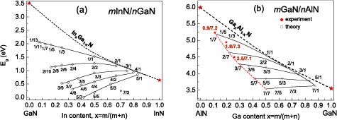
Figure 4. Calculated band gaps, Eg, for mInN/nGaN (a) and mGaN/nAlN (b) SLs versus chemical composition, x, compared with calculations performed for the corresponding InxGa1−xN and GaxAl1−xN alloys—the dashed curves. Free-standing growth mode is assumed, see explanation in section 4.2. Lines are fitted to the calculated values. Note a different scale for energy gaps in (a) and (b). Reprinted from [69], Copyright 2015, with permission from Elsevier. Experimental data in figure 4(b) are from [4].
Download figure:
Standard image High-resolution imageThe first observation is that only for the sets of m/1 SLs the band gaps are similar to Eg's of random alloys with the same effective composition x. Generally, the band gaps of SLs differ substantially from the gaps of the alloys. The concept of SLs enables to go far beyond the limitation of Eg evolution realized in ternary alloys. It is especially visible in the case of mInN/nGaN SLs, where calculations give Eg smaller than Eg of binary InN (0.65 eV). It takes place in several cases for m ⩾ 3 and the resulting metallization (closing of the effective band gap) occurs for m = n ⩾ 5. The latter effect was also demonstrated by Miao et al [70] where the possibility of the topological insulator formation was predicted.
Band gaps of mGaN/nAlN SLs in accordance with expectations, demonstrate much larger magnitude than Eg's of mInN/nGaN SLs. Their deviation from band gaps of GaxAl1−xN random alloy are much smaller than in case of In-containing SLs. For the 1/n, 2/n, and 3/n SLs Eg increases with increasing barrier thickness. For the set 5/n the gap is almost independent of n, while for the set 7/n there is a slightly decreasing dependence on n. Only for the 7/n type SLs band gaps smaller than the gap of pure GaN (3.6 eV) appear.
The calculated band gaps of mGaN/nAlN SLs (see figure 4(b)) are compared with the PL emission energies measured for 3 samples of SLs grown by MOVPE [4]. The declared layer thicknesses, m/n for these samples are: 0.9/7.2, 1.8/7.3, and 2.5/7.1 (non-integer m and n values reflect the fluctuations of the QW and QB layer thicknesses). The samples were grown pseudomorphically on an AlN substrate and the same pseudomorphic growth conditions were assumed in the calculations. As shown in figure 4(b), a very good agreement is obtained between the calculated Eg and the emission energies measured on the set of samples.
The results for InN/GaN cannot be compared to experimental data. Earlier published experimental data for samples of nominal 1InN/nGaN SLs [71] likely represent SLs with InGaN alloy in a QW. It was found [11] that their real composition was 1In0.33Ga0.67N/nGaN. Indium incorporation lower than 100% in the QW may be a general property for all 'InN ML' samples presented so far. The results for the InxGa1−xN/nGaN SLs will be presented and discussed in section 6.
To discuss further the band gap engineering in nitride SLs, an example of mInN/nGaN SLs will be used. Instead of using rather complicated dependence of Eg on the effective In/Ga content (which was useful for comparison of SLs and alloys), we plot the band gaps as functions of barrier and well thicknesses, i.e. n and m. Such a choice corresponds to the growth related approach.
Analysing the Eg dependence on QB and QW thickness, presented in figures 5(a) and (b), respectively, one observes that the band gaps are more sensitive to the well thickness than to the barrier width. Regarding the dependence on barrier thickness (figure 5(a)) the Eg at first (for m = 1) increases rapidly up to n = 5, then saturates. In contrast, for SLs with more than one InN ML the band gap decreases with increasing well and barrier thickness. As it is shown in figure 5(b), Eg decreases strongly with increasing well thickness and this dependence is more pronounced for larger n values. The crossover from increasing to decreasing trend occurring already for well width m = 2 (figure 5(a)) is clearly seen in figure 5(b).
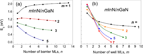
Figure 5. Calculated band gaps, Eg, for mInN/nGaN SLs versus barrier (a) and well (b) thicknesses expressed in number of MLs. Free-standing growth mode is assumed, see explanation in section 4.2.
Download figure:
Standard image High-resolution image4.2. Eg dependence on internal strain
To study the influence of the internal strain on Eg, we can simulate different strain conditions. The SL can be grown pseudomorphically on a substrate, thus having fixed in-plane lattice constant equal to the substrate lattice parameter. In this mode, the relaxation of the SL geometry is performed along the growth direction. The other strain mode corresponds to free-standing structure and involves a full relaxation of the atomic positions and lattice parameters.
In the case of the growth of In(Ga)N/GaN quantum structures, the QWs are strongly strained due to 10.6% of lattice mismatch between InN and GaN. Depending on the layer thicknesses and growth conditions, a relaxation of In(Ga)N can take place. It occurs when a thickness of indium containing layers exceeds so called critical thickness. To answer the question how the internal strain in InN wells influences the Eg values, two cases of growth conditions are compared: the pseudomorphic one, in which a-lattice constants of InN match to GaN and the free-standing one (a-lattice constant of the SL is an average of InN and GaN).
The InN/GaN band gaps presented in figures 4(a) and 5 were obtained assuming the free-standing, F-S, conditions, but some of the calculations for InN/GaN SLs were performed also for the case in which the SL is grown pseudomorphically on GaN substrate, which was motivated by the fact that In(Ga)N/GaN structures are often grown on bulk GaN substrate.
Figure 6 shows the calculated band gaps versus layer thicknesses for sets of mInN/nGaN SLs in the F-S mode and in the pseudomorphic strain mode. One can observe that all trends in the gap evolution are the same. However, the Eg values are generally smaller in the pseudomorphic mode, where closing of the gap occurs already for m = n ⩾ 4. In the case of 1/n SLs the difference between both strain modes is very small, but becoming larger for thicker wells, and it is quite pronounced for 5/n SLs (up to 0.5 eV). It reflects the influence of strain coming from the InN–GaN lattice mismatch on the InN layers, which causes the increasing degree of atomic relaxation along the growth direction.

Figure 6. Calculated band gaps, Eg, for mInN/nGaN SLs versus barrier thickness in the free-standing (dashed lines) and pseudomorphic (solid lines) strain mode.
Download figure:
Standard image High-resolution imageTo get a deeper insight into the problem of internal strain, the calculated atomic positions in three different strain modes are shown in figure 7 for 2InN/2GaN SL.
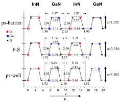
Figure 7. Bonds in 2InN/2GaN SLs in various strain modes: 'ps-barrier', 'F-S' and 'ps-well', see explanation in the text. Open symbols and dashed lines correspond to the corresponding bulk materials. All values are in Å. Reprinted from [69], Copyright 2015, with permission from Elsevier.
Download figure:
Standard image High-resolution imageIn the case of pseudomorphic growth to match the GaN barrier, called 'ps-barrier', InN layer is compressed to match the lattice a-constant of GaN. Consequently, the InN layer is thicker (c parameter larger). Opposite, in the case of pseudomorphic growth on InN, 'ps-well', the GaN layer is expanded to match the lattice constant of InN, which is larger and it results in thinner GaN layer (smaller c parameter). In the free-standing, 'F-S' case, the InN layer is somewhat compressed and GaN expanded, leading to an intermediate c value. The calculated bond lengths and lattice parameters are compared to the atomic positions and bond lengths in the corresponding InN and GaN bulk materials.
We can observe similar bond lengths in all the strain modes, but different angles between them. The next observation is that the effect of strain is larger in the InN well (layer thicknesses are changing from 5.70 Å to 5.87 Å) than in the GaN barrier (layer thicknesses change from 5.09 Å to 5.17 Å). It could be explained by 'softer' InN bonds. The band gaps of 2InN/2GaN SLs being affected mainly by the InN well geometry, change from 1.09 eV in the 'ps-barrier' strain mode to 1.27 eV in the 'F-S' mode and to 1.36 eV in the 'ps-well' growth case.
Concluding, the effects of lattice relaxation and internal strain are quite significant in InN/GaN SLs, due to large lattice mismatch (calculated values of the a lattice parameter of GaN and InN are 3.155 Å and 3.502 Å, respectively). We can compare this result for InN/GaN SLs with the case of GaN/AlN SLs, where the Eg variations with the different strain conditions are almost negligible (not exceeding 0.05 eV) [72] because of small lattice mismatch (calculated values of the a lattice constant are: 3.101 Å in AlN and 3.155 Å in GaN).
4.3. Built-in electric field
The fact that all the trends in evolution of the band gaps with barrier thickness (see figure 6) are the same, independent of the built-in strain, enables us to eliminate the strain effect from further discussion. Now, for a given strain mode, the band gap evolution may be analysed in terms of two counteracting effects: (i) the hybridization of QW and QB wave functions and (ii) the built-in electric fields. The overall SL band gap corresponds to the local Eg of the InN ML. The band gaps in SLs with thin QWs are dominated by the hybridization effect, which leads to a larger gap, due to the influence of the QB wave functions on the states in the QW. In 1/n SLs, contributions to the QW wave functions coming from GaN barrier cause an increase of the Eg from 0.65 eV (bulk InN) to about 2.1 eV in the InN well. Strong influence of the wave functions of GaN QB on the states in InN QW is observed up to n = 5, then Eg is almost constant, increasing very slowly. On the other hand, in SLs with wider QWs, the effect of the internal field dominates, leading to the reduction of the Eg values.
Wurtzite InN/GaN quantum structures grown along polar [0 0 0 1] axis are characterized by large polarization fields due to the spontaneous part and the piezoelectric polarization, the latter caused by lattice mismatch between QW and QB layers. The total polarization induces an internal electric field whose influence on the band profiles leads to the reduction of the electron–hole wave functions overlap. It results in a strong lowering of the radiative recombination rates and, consequently, the efficiency of optoelectronic devices, both laser diodes LDs and light emitting diodes LEDs drop down. A red-shift of the emitted light is observed. All the above mentioned effects constitute the so-called quantum confined Stark effect.
There are different theoretical methods to estimate the strength of the built-in electric field in SLs. Three of them will be presented below: (i) electric field, E, simply estimated from the slope of the band profile, (ii) E calculated by using the N-1s core-states as reference energies, and (iii) E estimated from polarization properties of bulk constituents. Below we will discuss the results for InN/GaN and GaN/AlN SLs obtained by these methods.
4.3.1. Electric field estimated from the band profiles.
Analyzing the band profiles one can estimate the strengths of the internal electric fields from the slopes of the profile curves. As an example, figure 8 shows band profiles with internal electric field directed from the type A interface towards the type B interface in both well and barrier regions in 5InN/5GaN SL. The different characters of the A and B interfaces and strong effect of the internal electric field are clearly seen. The strength of the electric field can be estimated from a linear approximation to the band profiles inside the QW and QB. The obtained values are: Eel = −6.6 MV cm−1 in the InN layers and Eel = 7.7 MV cm−1 in the GaN layers. The gap is indirect in real space and equal to Eg = 0.25 eV. The valence band offset, VBO, equal to difference between the valence band maxima in the central layers of InN well and GaN barrier, is estimated to be about 0.5 eV.

Figure 8. The valence- and conduction-band edge profiles in the 5InN/5GaN SL. Two non-equivalent interfaces, A and B, are indicated. Reprinted with permission from [72]. Copyright 2012 American Chemical Society.
Download figure:
Standard image High-resolution image4.3.2. Electric field calculated using the N-1s core-states as reference.
Values of the internal electric fields can be found from the ab initio calculations by using the N-1s core-states as reference energies. In figure 9, the energies of N-1s core-states, E1s, within layers of the 5/5 SL, are plotted along the [0 0 0 1] growth direction (polar c-axis). The N-1s energy values are different in successive MLs of the SL due to the presence of the induced electric fields. The magnitude of the internal electric field can be found from the slope of the best straight-line fit. The obtained values are: Eel = −7.0 MV cm−1 in InN well and Eel = 8.2 MV cm−1 in GaN barrier. These values are slightly higher than the values estimated from the band profiles presented in figure 8.
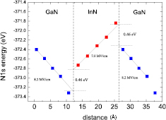
Figure 9. The N-1s state energies in subsequent layers of 5InN/5GaN SL along the growth direction. Reprinted with permission from [72]. Copyright 2012 American Chemical Society.
Download figure:
Standard image High-resolution imageThe VBO can be determined by the procedure described in [72], following the method used by Picozzi et al [73]. The VBO in this method is defined as: EVBO = ▵EI + ▵EB, where ▵EI is so called 'interface term' being the difference between the N-1s core-states energies in the QW and QB layers, and ▵EB is the 'bulk term' being the difference between N-1s state energies with respect to the valence band maxima in bulk QW and QB materials. ▵EI = 0.46 eV is found by extrapolation, as illustrated in figure 9. The calculated ▵EB term is: ▵EB = 0.10 eV. Thus our calculated VBO for 5InN/5GaN SL is equal: EVBO = 0.56 eV. This value is close to the one obtained by Moses et al [74] (0.62 eV) and it is in a good agreement with the experimental data (0.58 eV [75], 0.78 eV [76] and 0.8 ± 0.1 eV [77]).
The electric fields in wells and barriers of mInN/nGaN SLs are illustrated on figures 10(a) and (b), respectively. The internal Eel is ill defined in QW or QB thinner than 3 MLs. The first observation is that the electric field, both in InN well and inside the GaN barrier, depends strongly and almost linearly on the effective In composition. In InN well, the absolute values of the internal electric field decrease with increasing In content from 13 MV cm−1 for 3/7 SL down to 0.2 MV cm−1 for 7/1 SL. In GaN barrier, it increases with increasing In content from 0.9 MV cm−1 for 1/13 SL up to 14.8 MV cm−1 for 7/3 SL. The second observation is that the electric field values obtained for the given effective In composition (x = m/(m + n)) are slightly different for different layer thicknesses. As an example, we can consider the sequence of 3/3, 4/4, 5/5 SLs (x = 0.5). Comparing the electric field values for this set, we observe the general trend that internal electric fields, both in QWs and QBs, decrease with increasing number of MLs. Due to this trend we expect in 6/6 SL lower values of the electric field than in 5/5 SL. However, the influence of the electric field on the Eg values depends also on QW thickness, and despite the weaker electric field in the 6/6 SL, the overall band gap is even smaller than in the 5/5 SL due to the thicker QW and we observe closing of the gap (metallization).
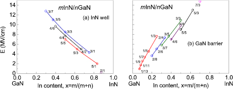
Figure 10. Absolute values of built-in electric fields in InN well (a) and in GaN barrier (b) of mInN/nGaN SLs as functions of effective In content. Lines are connecting the series of SLs with constant m. Reprinted from [69], Copyright 2015, with permission from Elsevier.
Download figure:
Standard image High-resolution image4.3.3. Electric field estimated using a semi-macroscopic model.
A semi-macroscopic model where the built-in electric fields in the QWs and QBs of the SL can be obtained from the spontaneous polarization and piezoelectric constants of the corresponding bulk materials, enables to analyze easily the electric fields in SLs for all the compositions and layer widths. The basic equations describing the electric fields: Ew in a QW and Eb in a QB are [78]:
where Pw and, Pb denote the polarizations in QW and QB, Lw and Lb are the QW and the QB thicknesses, λw and λb are the static dielectric constants of the well and barrier bulk materials.
The polarization contains spontaneous and piezoelectric parts (the (w,b) subscripts are omitted):

where Ppz originates from the distortions due to the lattice mismatch between quantum layers. Psp values for bulk materials are given in table 2, whereas Ppz is expressed by [79]:


where a and as are the lattice constants of QW or QB bulk material and the substrate, respectively.
Table 2. The spontaneous polarization, Psp (in C m−2), piezoelectric, eij, elastic, cij, and dielectric, λ, constants used in the model calculations.
| InN | AlN | GaN | |
|---|---|---|---|
| a (Å) | 3.533 | 3.112 | 3.186 |
| Psp | −0.035 [79] | −0.095 [79] | −0.027 [79] |
| λ | 15.3 [80] | 8.5 [80] | 10.4 [80] |
| e31 | −0.59 [8] | −0.67 [8] | −0.44 [8] |
| e33 | 1.14 [8] | 1.67 [8] | 0.75 [8] |
| c13 | 95 [81] | 115 [81] | 117 [81] |
| c33 | 235 [81] | 372 [81] | 400 [81] |
We use the described model to get the electric field strengths for InN/GaN and GaN/AlN SLs. The values of parameters used in the calculations are presented in table 2.
Figure 11 presents the calculated buit-in electric fields in QWs and QBs of mInN/nGaN (a) and mGaN/nAlN (b) SLs, as functions of the effective composition, x. We observe that, the electric fields are larger in mInN/nGaN than in mGaN/nAlN SLs, reaching 18.3 MV cm−1 in the barrier of 7InN/1GaN and 12.5 MV cm−1 in the barrier of 7GaN/1AlN SL. Larger values of built-in electric fields in mInN/nGaN than in mGaN/nAlN SLs are correlated with the larger lattice mismatch between InN and GaN than between GaN and AlN.

Figure 11. Electric fields in mInN/nGaN (a) and in mGaN/nAlN (b) SLs as functions of effective cation content, obtained from the 'model '(solid lines) and 'ab initio' calculations (open circles and dashed lines).
Download figure:
Standard image High-resolution imageThe described model neglects the atomistic structure of the SL structure; the resulting values of electric fields depend on the effective chemical composition (m/n ratio), as follows from equations (1) and (2)), but not on the separate values of m and n (like in ab initio calculations). This originates from using parameters of the bulk materials constituting the SL and neglecting specific SL features. Neverthless, the agreement between 'model' and 'ab initio' calculated values of Ew and Eb is quite good, as we can see from the comparison presented in figure 11. An advantage of the model calculations is that it easily provides the electric field strengths for any values of the QW and QB thicknesses, whereas, by ab initio calculations, we cannot obtain the internal electric field values for very thin layers (<3 MLs) and also for rather thick layers (>10 MLs) due to computational restrictions.
The dependence of the band gaps on both, wave function hybridization and built-in electric fields will be discussed in the next sections.
4.4. Wave functions hybridization
The selected structure for analyzing the contribution of the wave functions hybridization to the evolution of the band gap will be 1InN/5GaN SL.
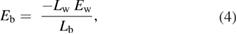
In figure 12 the total density of states (DOS), the valence and conduction band profiles, and the valence charge density through the MLs of 1InN/5GaN SL are shown. The band-edge profiles are characteristic for the presence of the internal electric field. Two kinds of interfaces are observed: A—interface (between the last Ga layer in the GaN2 barrier and the N layer in InN1 well), and B—interface (between the In layer in the InN1 well and the adjacent N layer in the GaN6 barrier). At the interface A the valence band maximum,VBM, is in the highest energetic position, whereas at the interface B the conduction band minimum, CBM, is in the lowest position. Spatial separation of the CBM and VBM results in the band gap indirect in real space and with reduced magnitude. It is interesting to note that despite the band gap lowering due to the effect of internal electric field, the value of Eg, about 1.95 eV is significantly larger than that of bulk InN, i.e. 0.7 eV. This effect is caused by hybridization of the InN well and adjacent GaN barrier wave functions.
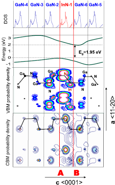
Figure 12. Evolutions of DOS, band-edge profiles, VBM and CBM charge density through the MLs of 1InN/5GaN SL. A and B denote two non-equivalent interfaces. Reprinted with permission from [82]. Copyright 2013, AIP Publishing LLC.
Download figure:
Standard image High-resolution imageSeparation of the VBM and CBM is reflected in an asymmetry of the charge distribution. We can see that charge is mainly localized on N sites, and interfaces A and B are not equivalent. The charge at the VBM is mainly accumulated at the interface A, in contrast, the CBM charge density is accumulated mainly at the interface B.
We observe also that the electron charge is more delocalized over the entire supercell, while localization near the InN ML mainly occurs for the hole states. Partly, this stems from the much smaller effective mass of the electrons compared to the holes. The calculations reveal an isotropically averaged effective masses for electrons of me = 0.171 and mhh = 1.118 for the heavy holes.
4.5. Competition between internal electric field and wave functions hybridization in the band gaps determination
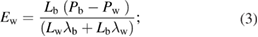
As was already mentioned, the Eg behavior in mInN/nGaN and mGaN/nAlN SLs, shown in figures 4–6 may be understood mainly in terms of the wave functions hybridization and the influence of built-in electric field. The SL band gap can be decomposed as:

where Eg(well) denotes the Eg of the bulk semiconductor forming the QW, ΔEg1 is the change of the Eg due to the internal electric field, and ΔEg2 includes the effects of hybridization of QW and QB wave functions, and also local atomic relaxations and strains from the substrate matching. ΔEg1 depends on the strength of the electric field and on the QW thickness:

In figure 13, the calculated electric fields (a) and ΔEg1 (b) as functions of barrier thickness are shown for mInN/nGaN SLs. We observe that the lowering of the SL band gaps for wider wells can be explained by the influence of the electric fields.
Figure 13. (a) Internal electric fields in wells and barrier of InN/GaN SL as functions of barrier thickness. Results of the model calculations (dots with lines) are compared for some cases with the ab initio calculated fields (open circles). (b) Energy gap shift, ΔEg1, due to the internal electric field.
Download figure:
Standard image High-resolution imageHaving determined ΔEg1 allows us to compare the mInN/nGaN and mGaN/nAlN band gaps (figure 4) with the gaps, Eg(hyp) for the hypothetical case corresponding to the internal electric field 'switched off', i.e.:

Figures 14(a) and (b) illustrate the band gaps Eg(hyp) for the two sets of 3/n and 5/n SLs in mInN/nGaN and mGaN/nAlN SLs, respectively. We observe that the Eg(hyp) are lying closer to the gaps of the corresponding random alloys than Eg(SL) and show an increasing trend as a function of the number n of barrier layers, in both mInN/nGaN and mGaN/nAlN SLs. Hence, we may conclude that the difference in Eg(SL) trends between these two systems (see also figures 4 and 5) is mainly due to the stronger internal fields in the QWs of mInN/nGaN SLs.

Figure 14. Calculated Eg(SL) (solid lines) in comparison with estimated Eg(hyp) (dashed lines) for mInN/nGaN (a) and mGaN/nAlN (b) SLs. Only two sets of SLs: 3/n and 5/n are considered. Note a different scale for energy gaps in (a) and (b). Reprinted from [69], Copyright 2015, with permission from Elsevier.
Download figure:
Standard image High-resolution imageAlmost constant values of Eg(SL) for both series 3/n and 5/n in mGaN/nAlN SLs illustrates the compensation between the effects of the internal field and the hybridization as the barrier width n is varied. As a numerical example, we can consider the 5GaN/7AlN SL, where the estimated reduction of the gap due to the electric field is ΔEg1 = −0.8 eV. Thus, Eg(SL) = 3.85 eV is decomposed into Eg(GaN) = 3.50 eV, ΔEg1 = −0.8 eV and ΔEg2 = +1.15 eV, i.e. ΔEg2 is larger than ΔEg1 originating from the internal electric field. On the other hand, for 5InN/7GaN SL we have Eg(SL) = 0.05 eV, Eg(InN) = 0.7 eV, ΔEg1 = −1.2 eV, and hence ΔEg2 = +0.55 eV. In this case, the contribution from the electric field dominates over that from the strain and hybridization effect.
Generally we observe that the gap evolution in thin well SLs is dominated by the hybridization effect, i.e. a wider barrier (larger n) leads to a larger value of Eg. In contrast, in SLs with wider wells the effect of built-in electric fields dominates influencing the band profiles and causing the band gaps to be indirect in real space, reduced in size, and eventually to vanish. This effect is larger in InN/GaN SLs than in GaN/AlN SLs, due to the stronger internal electric fields due to the larger piezoelectric part of polarization. More details can be found in [69].
4.5.1. Oscillator strength.
Both effects (i) overlap reduction between hole and electron states in the valence and conduction bands caused by the presence of electric field and (ii) weakening of the wave functions hybridization with increasing barrier thickness, result in a decrease not only the Eg values, i.e. PL energy emission, but also the PL intensity. We can connect the PL intensity with the overlap integral between the electron and hole wave functions, the square of which reflects the oscillator strength (OS) of a band-to-band transition. Experimentally, it is related to the intensity of both a light absorption and PL.
Figure 15 shows the ratio of transition matrix elements of edge transitions for SL and bulk GaN. The OS values for different structures were obtained from an implementation of the projector augmented wave (PAW) method [83] in an existing plane-wave code supporting non norm-conserving Vanderbilt-type ultra-soft pseudopotentials [84], i.e. the Vienna ab initio simulation package VASP [17]. Based on the corresponding PAW-derived all electron wave functions, an implementation of the optical matrix elements in the VASP package is developed. The optical transition matrix elements are given by:
where εi, εj are the single-particle energies, me is the mass of an electron,  is the reduced Planck constant,
  ,
,  are the conduction and the valence wave functions, respectively, and
  is the position operator. In this formulation, excitonic effects are neglected. The details of this model can be found in [85].
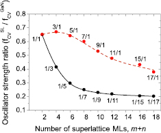
Figure 15. Relative OS of various 1InN/nGaN (in black) and mInN/1GaN SLs (in red) SLs with respect to bulk GaN as a function of SL period thickness m + n.
Download figure:
Standard image High-resolution imageAs one can see from figure 15, the highest electron–hole transition probability, i.e. OS, is found for the set of SLs with the shortest barrier, n = 1. OS is almost the same for very thin wells, but from m = 5, it starts to decrease. For thin wells, it can be explained by a weak effect of the electric field and strong well-barrier wave functions hybridization, whereas, for thicker wells, influence of the electric field is dominant reducing the OS. On the other hand, considering SLs with the single ML in the well (m = 1), a strong reduction of the wave functions hybridization occurs with increasing barrier thickness. It causes rapid reduction of the OS at the beginning, and then for thicker barriers, starting from around n = 5, the transition rates show tendency to saturate (around n = 15 the oscillator strength is around 20% of the bulk GaN value). This saturation results from the finite penetration lengths of electron and hole states into the SL barrier (an area in the GaN barrier begins to emerge wherein overlap between hole and electron states is approximately zero).
Concluding, we demonstrated that the effect of wave functions hybridization in SLs is dominant for narrow wells, whereas for wider wells, the effect of internal electric field is more important. We predicted theoretically that the PL emission intensity should drop with the increasing widths of SL layers, especially with QB thickness, as was shown for GaN/AlN SLs [86]. Unfortunately, experimental confirmation for InN/GaN SLs is not possible, due to the lack of structures with binary InN QWs. It seems that large lattice mismatch between InN and GaN as well as low structural stability of InN requiring significantly lower growth temperature make the task of obtaining InN/GaN SL very challenging.
5. Semipolar and nonpolar mInN/nGaN SLs
The electric fields reduce the overlap of the electron–hole wave functions and lowers the related radiative recombination rates. Consequently, the efficiency of optoelectronic devices, both LDs and LEDs drops down [87–89]. One way to reduce or even eliminate the internal electric field is to grow the quantum-well structures and related emitters along the semipolar or nonpolar m and a directions. The hexagonal unit cell of the wurtzite structure with indicated polar and nonpolar planes and corresponding growth directions is presented in figure 16.
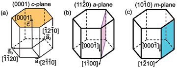
Figure 16. Sketch of the polar (a) and nonpolar-a (b) and nonpolar-m (c) crystallographic planes in the wurtzite structure.
Download figure:
Standard image High-resolution imageAlready in 2000 it was demonstrated [90] that epitaxial growth of GaN/AlGaN in a nonpolar direction allows fabrication of quantum structures free of electrostatic fields, with an improved optical efficiency. Nonpolar and semipolar InGaN/GaN laser diodes were demonstrated already, see for example [91–94]. Beside the application oriented studies, one observes also a growing interest within the nitride community in the fundamental properties of such structures. It motivates theoretical investigations of semi- and non-polar SLs.
5.1. Nonpolar mInN/nGaN SLs
The band structures of nonpolar mInN/nGaN SLs were investigated for two possible growth directions, along the a  and m
and m  axes. Arrangements of atomic MLs along these directions are illustrated in figure 17 for the example of 2InN/2GaN SL. In the case of SL grown in the a-direction, all the MLs are separated by the same distance a/2, where a is the lattice constant perpendicular to the c-plane, whereas MLs of SL grown in the m-direction can be separated by about 0.29a or 0.58a, and consequently two non-equivalent arrangements of MLs are possible. We call them m1 and m2.

Figure 17. Positions of MLs in 2InN/2GaN SLs grown in m and a directions in projection to the x-y plane. In atoms are indicated by red dots and Ga by open black circles. The corresponding anions are shifted in z direction. For the m growth direction, two possible arrangements of atoms: m1 and m2 are shown. The values of x and y are in units of the lattice parameter a. Reprinted with permission from [82]. Copyright 2013, AIP Publishing LLC.
Download figure:
Standard image High-resolution imageFigure 18 shows the relaxed atomic positions in 2InN/2GaN SLs for the three cases: a, m1, and m2. We observe that the relaxation of the atomic coordinates is different in the m1 and m2 case. The bond lengths are shorter in the m2 case inside the GaN layers and slightly longer inside the InN layers than in the m1 case.
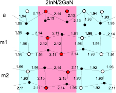
Figure 18. Relaxed positions of atoms in 2InN/2GaN SLs grown in a direction and in m direction with two arrangements of atoms (m1 and m2). In atoms are indicated by red dots, Ga atoms by open circles, and N by smaller black dots. Reprinted with permission from [82]. Copyright 2013, AIP Publishing LLC.
Download figure:
Standard image High-resolution imageThe calculated variations of the band gaps with effective In composition are presented in figure 19 for mInN/nGaN SLs grown in the a-direction (a) and the m-direction (b). Comparison with the band gaps of polar SLs (grown in the c-direction) is shown in figure 19(a). The dashed lines in figure 19 represent the calculations for InxGa1−xN alloys with a quasi-random ('uniform') cation distribution [64–66].
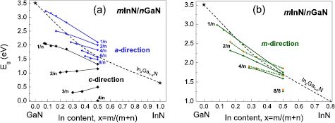
Figure 19. Calculated band gaps of mInN/nGaN SLs grown in nonpolar a direction (a) and m direction (b). Comparison with polar SLs is made and two arrangements of atomic MLs are indicated (m1-solid, m2-dotted lines). The dashed curves are fitted to the calculated gaps of InxGa1−xN quasi-random alloys [29, 30] and binary compounds, GaN and InN [31]. Reprinted with permission from [82]. Copyright 2013, AIP Publishing LLC.
Download figure:
Standard image High-resolution imageFigure 19 shows that all the observed trends are alike for the a- and m- growth directions: Eg increases with increasing barrier thickness (n) and decreases with increasing well thickness (m) reflecting (as in the case of alloys) the dependence of Eg on composition. This tendency is in the case of polar SLs valid only for m = 1, whereas, for higher values of m, Eg decreases also with increasing barrier thickness (n). All the gaps of the nonpolar SLs are lying rather close to the curve for random InxGa1−xN alloys (dashed lines),whereas they are much smaller in the polar case. We observe also that the gaps of SLs grown in the a direction (figure 19(a)) tend to be slightly larger than those of the SLs grown in the m-direction (figure 19(b)), illustrating the dependence of Eg on SL geometry, but the band gaps depend not only on the growth direction (a or m) of SL, but also on the atomic arrangement (m1 or m2) for the m growth direction. Two possible arrangements of atomic layers for even/even SLs grown in the m direction lead to different values of the band gaps (represented by solid and dotted lines).
As already discussed, the low values of the band gaps in polar SLs originate from the strong internal electric fields present in these structures, which determines the effective Eg. The electric field leads to a spatial separation of the VBM and CBM density of states. Consequently, the 'indirect in real space' band gap becomes very small for thick layers. In contrast, in nonpolar SLs, grown along the a- or m-axis of the wurtzite structure, there is no macroscopic polarization and no internal electric field. Polar and nonpolar SPLs with the same composition show difference in the band gap values above 1 eV. A similar energy difference arises when we 'switch off' the electric field in polar SLs (see figure 14(a)).
In figure 20, band gaps of 3InN/nGaN SLs are presented for 3 growth directions, a, m and c, and compared to hypotetical band gaps of c-SLs with 'switched off' electric field. We observe that indeed differences in the band gaps between polar and nonpolar SLs come mainly from the existence of electric field in polar structures, but the effect of geometry itself has to be taken into account also.

Figure 20. Calculated band gaps of 3InN/nGaN SLs for three growth directions, a, m and c, compared to hypotetical band gaps of c-SLs with switched off electric field (dashed line).
Download figure:
Standard image High-resolution imageThe relaxed atomic geometries, the valence and conduction band profiles, and the probability densities for the VBM and CBM states through the 1InN/5GaN MLs are illustrated in figures 21(a) and (b), for the a-, and m-growth orientations, respectively. Figure 21 shows that the charge distribution along the growth direction is significantly different for nonpolar SLs and polar (see figure 12) SLs. In the absence of an internal electric field, the band profiles are flat, the band gap is 'direct in real space' and significantly larger (3.05 eV—a direction, 2.75 eV—m direction) than in the polar case (1.95 eV). Also, there is no noticeable charge transfer between the layers. The relaxation of atomic positions leads to In–N bond lengths slightly shorter than in pure InN, but different for a and m cases due to different geometry of the supercell.

Figure 21. Relaxed positions of atoms (in Å)—top, band-edge profiles—middle, and band-edge electron densities—bottom, through MLs of 1InN/5GaN SL grown in a-direction (a), and m-direction (b). A and B denote two different interfaces. The gray areas represent planes shifted up by 0.8 Å in (a) and 1.6 Å in (b). Reprinted with permission from [82]. Copyright 2013, AIP Publishing LLC.
Download figure:
Standard image High-resolution imageIn conclusion, comparing the Eg behavior for three differently oriented SLs, two aspects should have been in focus: the influence of internal electric fields (comparison of polar and nonpolar SLs) and the dependence on lattice geometry (comparison of a-and m-oriented nonpolar SLs). It is interesting to note that the band gaps depend not only on the growth direction and the widths of the layers, but also on the arrangements of layers, and atomic positions inside the layers. This was illustrated by the band gaps in two different types of InN/GaN SLs grown in the m direction.
As has been discussed for a variety of semiconductors, the pressure coeficient of the band gap dEg/dp supplies an important information about mechanisms controlling a behavior of the band gap [95]. In particular, in the case of polar nitride quantum structures dEg/dp exhibits a significant reduction with respect to the alloys with equivalent composition [96]. The internal electric field present in quantum structures is responsible for this effect. In this context it is interesting to study the dependence of dEg/dp on the growth directions. The calculated dEg/dp for selected polar and nonpolar SLs is shown in figure 22. One can see that, in agreement with expectations, the band gap pressure coefficients in nonpolar SLs are lying very close to the curve presenting dEg/dp obtained for InxGa1−xN quasi-random alloys and close to the InN band gap pressure coefficient (28 meV GPa−1). In contrast, dEg/dp calculated for polar mInN/nGaN SLs [71] have significantly lower values, which decrease further with QW (m), and QB thickness (n). The gaps and their pressure coefficients for nonpolar SLs (especially those grown in the m direction) vary with composition in a similar fashion as those calculated for 'bulk' InxGa1−xN alloys.

Figure 22. Calculated band gap pressure coefficients, dEg/dp, for nonpolar 1InN/nGaN SLs grown along the a- and m-directions in comparison with the dEg/dp calculated for polar SLs [19]. Results of the calculations performed for InxGa1−xN quasi-random alloys are represented by the dashed curve. [97] John Wiley & Sons. Copyright © 2014 WILEY-VCH Verlag GmbH & Co. KGaA, Weinheim.
Download figure:
Standard image High-resolution imageMore details on the nonpolar SLs can be found in [97].
5.2. Semipolar mInN/nGaN SLs
Significant efforts during the last 15 years have been devoted to studies of semipolar nitride quantum structures and devices [10, 70, 93, 98]. It is interesting to consider theoretically their electronic band structure and verify the expectation that their properties represent intermediate cases with respect to polar and nonpolar SLs.
There is a wide variety of the growth directions enabling realization of the semipolar type of structures. For the purpose of illustration, two selected cases will be used: SLs grown along the s2 and s6 directions. Figure 23 shows the hexagonal unit cell of the wurtzite structure with the s2-plane (a) and s6-plane (b) indicated. The s2-plane is defined by the orthogonal directions ![$\left[ 1\,\bar{1}\,0\,0 \right]$](https://content.cld.iop.org/journals/0953-8984/30/6/063001/revision2/cmaaa2aeieqn009.gif) and
and ![$\left[ 1\,1\,\bar{2}\,\bar{3} \right]$](https://content.cld.iop.org/journals/0953-8984/30/6/063001/revision2/cmaaa2aeieqn010.gif) , corresponding to the vectors
, corresponding to the vectors  and
and  (in terms of the lattice vectors shown in figure 23(a)). The s2 growth direction is then given by the direction of
  , which is along
  , in terms of the reciprocal lattice vectors
  . Similarly, the s6-plane, illustrated in figure 23(b), is defined by the orthogonal directions
 ![$\left[ 1\,\bar{2}\,1\,0 \right]$](https://content.cld.iop.org/journals/0953-8984/30/6/063001/revision2/cmaaa2aeieqn016.gif) and
and ![$\left[ 1\,0\,\bar{1}\,\bar{4} \right]$](https://content.cld.iop.org/journals/0953-8984/30/6/063001/revision2/cmaaa2aeieqn017.gif) , which correspond to the vectors
, which correspond to the vectors  and
and  , with the normal given by the direction of
  .
.

Figure 23. Sketch of the semipolar s2 and s6 crystallographic planes in the wurtzite structure.
Download figure:
Standard image High-resolution imageThe electronic structures of semipolar mInN/nGaN SLs have been calculated and compared to similar calculations for polar SLs (grown along the c-direction) and nonpolar SLs (grown along the a- and m-directions).
In figure 24, the relaxed atomic positions are shown through the MLs of the 1/5 SLs grown in the s2 (a) and s6 (b) directions. For the s2-SL, the constructed supercell contains two cations and two anions in one ML, whereas there are four cations and four anions in one ML in the s6-SL geometry, which lie at different coordinates along the growth direction leading to the formation of characteristic staggered interfaces [99, 100]. The average ML separation is indicated in figure 24, showing a local enhancement at the InN ML. In both cases (s2 and s6), the bonds in the vicinity of the interfaces A and B are generally shorter than in the corresponding binaries (InN: 2.15 Å, GaN: 1.95 Å). We observe also that the atomic relaxations are more complicated in the s6 case (the local bonds around the four cations within each ML are not identical).
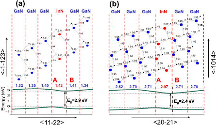
Figure 24. Top view of the relaxed atomic structure of the 1/5 SLs grown in the s2-direction (a), and the s6-direction (b) of the wurtzite structure. Only the atoms within the SL unit cell are shown. A and B denote two different interfaces. The bond lengths and ML widths are indicated (in Å). In the lower panel, the corresponding local valence- and conduction-band edges are traced through the SLs. Reprinted with permission from [101]. Copyright 2014, AIP Publishing LLC.
Download figure:
Standard image High-resolution imageIn the lower panel of figure 24, the valence and conduction band edges are traced through the SL showing typical band edge profiles of a SL with an internal electric field directed from the A interface towards the B interface in both QW and QB regions. The SL band gap ('indirect in real space') is the difference between the overall VBM (which is found at the InN layer at interface A) and the overall CBM (which is found at the InN layer at interface B). Its magnitude is Eg = 2.9 eV for the s2-SL and Eg = 2.4 eV for the s6-SL. The above results can be compared to the polar case where much stronger asymmetry in the bond lengths and charge distribution is leading to larger slopes of the band edge profiles and even smaller 'indirect' band gaps. Thus, semipolar SLs, with weaker influence of the electric field on the band structure than found for polar SLs, represent 'intermediate' case between polar and nonpolar SLs.
To further investigate the relation between the internal electric field and the band gap, the electric fields were estimated for several s2- and s6-SLs and compared with the values obtained for polar SLs. The electric field strengths were obtained by using the N-1s core-levels as reference energies by the procedure described in section 4.3.2. Examples of the obtained values of the electric field for semipolar and polar SLs are given in table 3. As it was already mentioned, it is not possible to find the electric field value for one or even two MLs. As it results from table 3, the electric field strengths are quite similar for the s2- and s6-SLs ranging from 1 MV cm−1 to 4.9 MV cm−1, but much smaller than those obtained for polar structures (between 3.6 MV cm−1 and 15.6 MV cm−1) for the same range of compositions.
Table 3. The values of the electric fields (in MV cm−1) in semipolar m/n SLs grown in s2 and s6 directions in comparison with the electric field values obtained for polar (c-direction) SLs (last two rows).
| m/n | 1/3 | 1/5 | 1/7 | 2/4 | 2/6 | 2/8 | 2/10 | 3/3 | 3/5 | 3/7 | 3/9 | 4/4 | 4/8 | 6/6 |
|---|---|---|---|---|---|---|---|---|---|---|---|---|---|---|
| InN–s2 | — | — | — | — | — | — | — | −4.0 | −4.6 | −4.9 | −5.4 | −3.4 | −6.1 | −2.3 |
| GaN–s2 | 3.0 | 1.3 | 1.0 | 3.0 | 2.3 | 1.8 | 4.5 | 2.9 | 2.2 | 4.2 | 2.5 | 2.9 | ||
| GaN–s6 | 3.8 | 2.1 | 3.7 | |||||||||||
| InN–c | — | — | — | −9.8 | −12.5 | −15.6 | ||||||||
| GaN–c | 8.1 | 5.0 | 3.6 | 7.5 | 5.2 | 3.8 | 11.6 | 9.4 | 8.5 | |||||
The calculated band gaps, Eg, versus In content, x = m/(m + n), for semipolar m/n s2-SLs are compared in figures 25(a) and (b) with those obtained for polar and nonpolar SLs. The calculated band gaps for semipolar s2-SLs are seen to fall slightly below the band gaps of SLs grown in the nonpolar a-direction (figure 25(a)), whereas the band gaps for semipolar s6-SLs are lying below the band gaps of SLs grown in the nonpolar m-direction (figure 25(b)). In all the semipolar and nonpolar SLs, the band gaps increase with barrier thickness, n, and decrease with well thickness, m. This behavior is in agreement with the intuitive expectations. On the other hand, in polar SLs such a trend is seen only for m = 1, the band gaps for m > 1 decrease both with increasing m and n values (see figures 4(a) and 5).
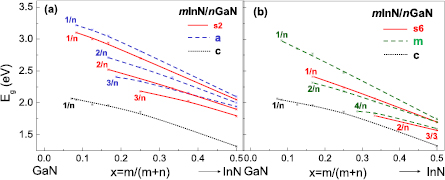
Figure 25. The calculated band gaps for semipolar s2 (a) and s6 (b) mInN/nGaN SLs in comparison with those calculated for nonpolar (a and m) SLs and polar (c) SLs. Reprinted with permission from [101]. Copyright 2014, AIP Publishing LLC.
Download figure:
Standard image High-resolution imageIn conclusion, studying different types of SLs two aspects have to be taken into account: the influence of internal electric fields (comparison of polar, semipolar, and nonpolar SLs) and the dependence on lattice geometry (comparison of nonpolar SLs in the a- and m-direction, as well as semipolar SLs in the s2- and s6-direction).
6. SLs containing nitride alloys
In the following we discuss the band gaps of short period mGaN/nGayAl1−yN, mInyGa1−yN/nGaN, mGaN/nInyA1−yN and mInyAl1−yN/nGaN SLs grown along the wurtzite c axis (polar structures) and we analyze the main factors influencing their behavior. The role of the built-in electric field and the hybridization of well and barrier wave functions is discussed in detail. The effects of internal strain and cation clustering are also taken into account. The discussion includes comparison with existing experimental data. It turned out that obtaining mInN/nGaN SLs is very difficult. There has been an increasing amount of structural studies which show that instead of intentionally introduced mInN QWs InxGa1−xN layers are grown in such structures. Using both growth method MOVPE or MBE structures with x not larger than 0.4 are obtained. The photoemission energies for mInxGa1−xN/nGaN SLs with given In content, x, and layer widths, m and n are compared with the calculated band gaps for these SLs.
6.1. mInyGa1−yN/nGaN and mGaN/nGayAl1−yN
Figure 26(a) shows the calculated band gaps, Eg, for sets of mInyGa1−yN/nGaN SLs with three different compositions in the InyGa1−yN well: y = 0.25, 0.33 (one set, 1/n) and y = 0.5 (various choices of m/n). In figure 26(b) the gaps for mGaN/nGayAl1−yN with the composition in the GayAl1−yN barrier: y = 0.5 (selected sets m/n) and y = 0.67 (one set, m/1) are presented. The band gaps are shown as functions of effective cation composition in order to compare to the Eg's of the corresponding random alloys (InxGa1−xN and GaxAl1−xN). The calculated band gaps in both, the mInGaN/nGaN and mGaN/nGayAl1−yN SLs increase with increasing barrier thickness and decrease with increasing well thickness. They deviate from the Eg's of the corresponding alloys, especially for wider QWs and QBs. This effect is more pronounced in mInyGa1−yN/nGaN SLs.

Figure 26. Calculated band gaps, Eg, for mInyGa1−yN/nGaN (a) and mGaN/nGayAl1−yN (b) SLs versus the effective In (Ga) cation fraction, x, compared with calculations performed for the corresponding random alloys (dashed curves) [64]. For mInyGa1−yN/nGaN the calculated gaps are compared with the experimental data obtained for the set of 1In0.33Ga0.67N/nGaN SLs (red dots) [11]. Lines are spline fits to the calculated values. Different scales in (a) and (b) are used in order to obtain sufficient resolution. Reprinted with permission from [102]. Copyright 2015, AIP Publishing LLC.
Download figure:
Standard image High-resolution imageAnalysing figure 26(a) we observe that the calculated band gaps for 1InyGa1−yN/nGaN SLs with lower y (y = 0.25 and 0.33) are significantly larger compared to the analogical set (1/n) of SLs with y = 0.5 and they are also lying much higher than the gaps of 1InN/nGaN SLs (see figure 4(a)). And even higher than the band gaps of the InxGa1−xN alloy. It can be explained by the fact, that for lower y, gaps are less affected by the internal electric field (decreasing the gaps) due to smaller lattice mismatch between QW and QB and more dominated by the hybridization effect which increases the Eg values.
The main factors influencing the band gap behavior will be discussed in more details in the next sections.
6.1.1. Comparison with experimental data.
The calculated band gaps are compared to PL energies measured on a set of 1In0.33Ga0.67N/nGaN samples with m/n = 1/2, 1/3, 1/4, 1/10, and 1/40 (red dots in figure 26(a)) [11]. Intentionally, these samples were grown as 1InN/nGaN short-period SLs [2], and it was believed that they contain one ML of pure InN. Consequently, the previous theoretical works [72, 103, 104] on InN/GaN SL indicated on significant discrepancy between theory and experiment. The calculated 1InN/nGaN band gaps were about 1 eV lower than the PL energies measured on the mentioned samples.
Several hypotheses were proposed to explain this discrepancy, including the suggestion that optical transitions are due to GaN excitons partially localized in the InN region [11], or that the observed light emission originates from the recombination of carriers located in different spatial regions, i.e. from the GaN QB to the InN QW [25, 69] and that the observed discrepancy was caused by screening of the internal electric fields in the polar structures by free carriers originating from unintentional defects, an effect which was not included in the calculations [82]. The last hypothesis suggested that the inserted layer is not pure InN, but actually consists of an ternary InGaN alloy [70, 71, 99]. To check this hypothesis, quantitative high resolution transmission electron microscopy (TEM) studies were performed on the set of nominal 1InN/nGaN short-period SLs. It was revealed that the SLs consist of an InxGa1−xN ML with an indium content of x = 0.33 instead of the intended x = 1. Figure 26(a) shows that the calculated gaps of 1In0.33Ga0.67N/nGaN SLs are lying close to PL energies measured for the set of samples with In content corrected to the value y = 0.33. Lower In incorporation may be a general property for all 'InN-ML' samples presented so far. To make a further comparison between the experiment and theory, under the assumption that the SL samples studied have an 1In0.33Ga0.67N/nGaN structure, we performed calculations of the Eg dependence on pressure. The results are compared in figure 27 to the experimental data obtained from the PL measurements under pressure for three investigated 1/n SL structures (1/3, 1/10, 1/40) [71]. The measured pressure coefficients, dEPL/dp, range from 33.4 meV Gpa−1 to 28.7 meV GPa−1 and are in a good agreement with the band gap pressure coefficients, dEg/dp, calculated for In0.33G0.67N/nGaN and In0.4G0.4N/nGaN SLs taking into account that the pressure coefficients are subject to appreciable error bars: ±1.5 meV GPa−1 in the experiment, and ±2 meV GPa−1 in the calculations. They show the same trend as observed in InxGa1−xN alloys approaching the InN band gap pressure coefficient (28 meV GPa−1) for higher In content. In contrast, dEg/dp calculated for 1InN/nGaN SLs. (see figure 27) have significantly lower values, which furthermore decrease with barrier thickness n.

Figure 27. Comparison of the calculated band gap pressure coefficients, dEg/dp, for 1In0.33Ga0.67N/nGaN, 1In0.4Ga0.6N/nGaN, 1In0.5Ga0.5N/nGaN and 1InN/nGaN SLs with the measured pressure coefficients of PL peak energies, dEPL/dp, for 1In0.33Ga0.67N/nGaN SLs (red dots). The values of n are indicated. The dashed curve presents the results of the calculations performed for InxGa1−xN quasi-random alloys [53, 105].
Download figure:
Standard image High-resolution imageAnother set of mInxGa1−xN/nGaN samples, that we can compare to was grown recently [13] by MOVPE technique. QW thicknesses were 1–4 MLs and In content, x, was in the range from 0.30 to 0.33. The results of PL measurements brought a new information on SL properties since the reported so far experimental results were obtained on SLs with 1 or 2 MLs in QW, only. Figure 28 shows the calculated band gaps of mIn033Ga0.67N/nGaN versus QB thickness for different values of m in comparison with PL emission energies obtained on the fabricated samples. Good agreement between theoretical and the experimental gaps is observed.

Figure 28. Calculated band gaps, Eg, for mIn033Ga0.67N/nGaN SLs versus barrier thickness, n, in comparison with experimental PL data obtained for mInxGa1−xN/nGaN samples with estimated x in the range: 0.30–0.33, blue dots correspond to m = 1, red dots are for m = 2, and green dot for m = 4. Dashed lines are extrapolations of the calculated Eg values for higher n values.
Download figure:
Standard image High-resolution imageAnalysing figure 28, we can see that the band gaps increase with increasing barrier thickness for all the considered well widths (up to = 5). Contrary to the case of binary mInN/nGaN SLs (figure 5(a)), we do not observe the change of the increasing trend observed for m = 1 to decreasing one, for m > 1, however, Eg increases more slowly for higher m values. We can interpret it in terms of much weaker, than in mInN/nGaN SLs, built-in electric field, which is sensitive to indium content, x, in QW. Higher In content leads to higher lattice mismatch between InGaN and GaN layers, resulting in increases the piezoelectric polarization and consequently the electric field strength.
6.1.2. Influence of electric field and wave function hybridization on the band gaps.
Due to the possibility of comparison with the experimental data, we will concentrate in our analysis on the mIn0.33Ga0.67N/nGaN SLs.
Figure 29 illustrates the internal electric fields in wells (Ew) and barriers (EB) of mIn0.33Ga0.67N/nGaN and mGaN/nAl0.33Ga0.67N SLs obtained from the model described in section 4.3.3. The fields are given as functions of the number of barrier MLs, n.
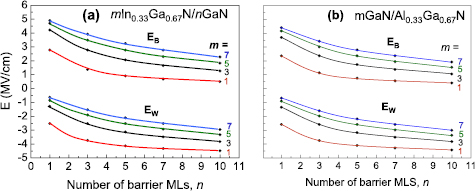
Figure 29. Electric fields in wells (Ew) and barriers (EB) of mIn0.33Ga0.67N/nGaN (a) and mGaN/nAl0.33Ga0.67N (b) SLs as functions of number of barrier MLs.
Download figure:
Standard image High-resolution imageConsidering Ew and EB dependence on n, one can distinguish two regions: thin QBs (n up to ~4 MLs) and thicker QBs (n > 5 MLs). In the 1st region, absolute values of the electric field strongly increase with n in QW and strongly decrease in QB. Then, in the 2nd region the dependence of the electric field on n becomes quite weak. The electric fields in mInyGa1−yN/nGaN are slightly higher than in mGaN/nGayAl1−yN SLs, which relates to the larger lattice mismatch (stronger piezoelectric contribution), and they are significantly lower than in mInN/nGaN SLs (see figure 13(a)).
As it was already shown in section 4.5, the SL band gap Eg(SL) may be decomposed as a sum: Eg(SL) = Eg(well) + ΔEg1 + ΔEg2, where Eg(well) denotes the band gap of the bulk QW material, ΔEg1 = eEdw is the reduction of EG due to the internal electric field, Eel, and ΔEg2 include the effects of strains, local atomic relaxations, and hybridization of well and barrier wave functions. In figure 30(a), the energy gap shift, ΔEg1, due to the internal electric field, is shown for the set of mIn0.33Ga0.67N/nGaN SLs. One can observe that ΔEg1 depends strongly on m and n values. The largest values of ΔEg1, are in SLs with wide QWs and QBs, where the influence of internal electric fields is dominant, whereas, in SLs with thin layers the hybridization of well and barrier wave functions is more significant. The highest estimated reduction of EG due to the electric field, ΔEg1 = −0.57 eV, is found for 7/10 SL.
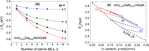
Figure 30. (a) Energy gap shift, ΔEg1, due to the internal electric field. [13] John Wiley & Sons. © 2017 WILEY-VCH Verlag GmbH & Co. KGaA, Weinheim. (b) comparison of the calculated SL band gaps, Eg(SL) (solid lines) with the hypothetical ones, Eg(hyp), (dashed lines) for three sets of mIn0.33Ga0.67N/nGaN SLs: 1/n, 3/n and 5/n.
Download figure:
Standard image High-resolution imageBy correcting the calculated band gaps for the effect of the electric field, one can obtain gaps, Eg(hyp), for the hypothetical case with the internal electric field 'switched off': Eg(hyp) = Eg(SL) − ΔEg1. They are shown in figure 30(b) for three sets of mIn0.33Ga0.67N/nGaN SLs: 1/n, 3/n and 5/n (solid lines) in comparison with the SL gaps, Eg(SL) (dashed lines).
It can be concluded from figure 30(b) that the Eg(hyp) are lying even higher compared to the gaps of the equivalent random alloy In0.33Ga067N than Eg(SL), which effect can be explained by strong wave function-hybridization effect in these SLs.
6.1.3. Oscillator strength.
Figure 31 shows the oscillator strength ratio of SL and bulk GaN for the set of 1InxGa1−xN/nGaN SLs with In content x = 0.33, 0.25 and 1. We observe that the oscillator strength ratio increases with decreasing In content in the QW, reaching the strength for 1In0.25Ga0.75N/1GaN SL almost equal 0.9. Also, the character of the dependence on barrier thickness changes drastically. Contrary to 1InN/nGaN SLs, in the 1In0.25Ga0.75N/1GaN and 1In0.33Ga0.67N/nGaN the dependence on layer thickness is quite weak for thin barriers and does not saturate so fast. In particular, the SLs 1/1 and 1/3 with x = 0.25 are characterized by almost the same oscillator strength ratio. It can be explained by much stronger penetration of well wave functions into the barrier region (especially for thin barriers) than could occur in the case of binary 1InN/nGaN SLs and also by lower strength of the internal electric fields.
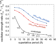
Figure 31. Oscillator strength ratio of SL and bulk GaN as a function of SL period thickness for different structures of 1InxGa1−xN/nGaN SLs with In content x = 0.25 and 0.33 in comparison with x = 1.
Download figure:
Standard image High-resolution image6.1.4. Influence of atomic arrangement on the band gaps—cation clustering.
The band structure calculations discussed in the previous section were performed in a supercell geometry modelling a uniform distribution of cations in the GaAlN and InGaN layers of the SL. In practical sample preparation, it is a severe issue whether ideal homogeneity of the random ternary alloys can be achieved, or rather regions of varying relative cation concentration are formed during growth (cation clustering). This may have significant bearings on the predictions of the properties of the SLs, as clustering tends to decrease the effective band gap of the random alloy.
The effects of cation clustering in nitride alloys were studied earlier [66, 67] and a noticeable lowering of the alloy band gap was demonstrated. Here, we undertake a similar study for the SLs.
In figure 32, the calculated band gaps of polar 1In0.33Ga0.67N/nGaN SLs for uniform and clustered arrangements of the In atoms in the InGaN QW are compared. Generally, the clustering can be realized in different ways as was already discussed in [66]. Here, we simulate 1In0.33Ga0.67N/nGaN SLs by 1In3Ga6N9/nGa6N9 supercell either by distributing three In atoms as uniformly as possible over the nine cation positions of the In3Ga6N9 QW or by clustering them together in one corner of the supercell layer. The dashed lines in figure 32 represent comparisons of the calculated [66] band gaps of InxGa1−xN alloys with those of a uniform and a clustered indium distribution.

Figure 32. Calculated band gaps, Eg, of In0.33Ga0.67N/nGaN SLs for two cases: uniform (blue open circles) and clustered arrangement of In atoms (green dots) in comparison with the experimental data (big red dots) [11]. The values of n are indicated for both experimental and theoretical data. Lines are spline fits to guide the eye. The dashed curves correspond to the calculations performed for InxGa1−xN alloys with uniform and clustered arrangements of In atoms [64]. Reprinted with permission from [102]. Copyright 2015, AIP Publishing LLC.
Download figure:
Standard image High-resolution imageThe band gaps of the SLs with clustered In-arrangements in the QW are substantially smaller than those obtained for the SLs with uniformly distributed In atoms. This observation is in agreement with the band gap behavior in alloys. The effect was explained on the basis of lattice relaxation and strong hybridization of In and N wave functions when the number of In atoms binding to a particular nitrogen atom exceeds the statistical average (which seems to be the definition of clustering) [66].
The Eg difference between the two SL models is smaller than for the equivalent alloys, which corroborates the observation that for a 1 ML well, the gap is to a large extent governed by the barrier. A similar comparison performed for sets of 1In0.25Ga0.75N/nGaN SLs (simulated by the 1In3Ga9N12/nGa12N12 supercell) shows that the band gaps for clustered arrangement of In ions are reduced by about 0.1 eV–0.15 eV with respect to those of the uniform arrangement.
It was suggested recently [106], that the uniform arrangement of In atoms in 1In0.33Ga0.67N/nGaN SL corresponds to a  ordered structure. As observed by experiment, for certain growth conditions, InxGa1−xN monolayers may self-organize into laterally ordered and periodic structures, which were identified as a
  reconstruction with a stoichiometry of In0.33Ga0.67N. With this new compositional information, the calculated band gaps are in excellent agreement with the measured photoluminescence data [11].
Specific role of In cations was demonstrated above. The observation that the band gaps of SLs with clustered In-arrangements in alloys are substantially smaller than those for the SLs with uniformly distributed In atoms is similar to the trend found for In-containing alloys.
6.2. mInyAl1−yN/nGaN
The InAlN band gap can be tuned from about 0.7 eV–6.2 eV. Due to such a large spectral range, quantum structures based on this material are very promising for applications. In this context, studies of band structure evolution in the system of the combined multilayers of InyAl1−yN and GaN forming SLs are interesting and important. The aim of this Section is to show that there is a number of physical problems which require a better understanding. Among them are: (i) expected strong internal strain and built-in electric field, both caused by large InN–AlN and InN–GaN lattice mismatches, (ii) interplay between spontaneous and piezoelectric polarizations (especially around y = 0.17–0.18, where InyAl1−yN is lattice-matched to GaN), (iii) properties of mInyAl1−yN/nGaN SLs with equal GaN and InyAl1−yN band gap values (3.5 eV) for y around 0.20; as a consequence, for y < 0.2, we deal with nGaN/mInyAl1−yN SL, whereas for y > 0.2, it is mInyAl1−yN/nGaN SL, according to the commonly used convention to denote QW/QB in a SL.
In figure 33, the calculated band gaps of mInyAl1−yN/nGaN SLs for y = 0.83, 0.67, 0.50, 0.33, and nGaN/mInyAl1−yN SLs with y = 0.17, 0.12 are shown for m = 1, as functions of the effective Ga composition n. This way of presentation enables a comparison with the quaternary alloys Iny(1−x) Al(1−y)(1−x)GaxN with the same effective contents of In, Al and Ga. More details can be found in [107], where the case m = 3 is considered also.

Figure 33. Calculated band gaps, Eg for 1InyAl1−yN/nGaN and nGaN/1InyAl1−yN SLs (solid lines) in comparison with Eg calculated for Iny(1−x)Al(1−y)(1−x)GaxN alloy (red dashed lines) with the same chemical composition. Experimental PL results for nGaN/1InyAl1−yN SLs are also indicated (blue star, dot and triangle), see description in the text.
Download figure:
Standard image High-resolution imageAnalysing the band gap behavior of both types of SLs (y-value either larger or lower than 0.2) we observe that for higher values of n their Eg approaches the GaN band gap (3.5 eV) from the opposite directions (increasing or decreasing with n). An exception is the mIn0.33Al0.67N/nGaN SL, where the band gap increases first, exceeding the bulk values of both of the constituents for n = 1, then decreases for higher n. As it is shown in figure 33, the band gaps of nGaN/mInyAl1−yN SLs agree well with these Iny(1−x) Al(1−y)(1−x)GaxN alloys with the same effective composition. On the other hand, Eg values of mInyAl1−yN/nGaN SLs show, especially for thicker barriers, significant deviations from the alloy band gaps. These differences come from the characteristic features of SLs, as built-in strain, internal electric fields and the wave functions hybridization, which will be discussed in the next subsections.
The calculated gaps are compared in figure 33 with PL emission energy measured on the samples with the same effective Ga composition, but different layer thicknesses. They are: 3GaN/3In0.12Al0.88N [108] (blue dot), 1GaN/7In0.18Al0.82N [8] (blue star) and 3GaN/7In0.18Al0.82N [8] (blue triangle). Experimental data for the first two samples are lying close to the calculated curves for SL with the same (or similar) In composition. Observed deviation for the third sample can be explained by the slightly different In composition and by the fact that layer thicknesses in the calculations are different from those in the measured samples. Taking the above into account, one can conclude that the agreement between experiment and calculations is quite reasonable.
6.2.1. Influence of internal strain on the SLs band gaps.
To illustrate the role of internal strain, the band gaps are calculated for SLs in two strain modes; pseudomorphic growth on a GaN substrate (ps-GaN), and pseudomorphic growth on InAlN substrate (ps-InAlN).
The obtained results for 1InyAl1−yN/nGaN SLs and nGaN/1InyAl1−yN SLs are presented in figure 34. The most pronounced difference in Eg values between the two strain modes, ΔEg = 0.52 eV, is found for SL with the largest In content, y = 0.67. It is caused by the large lattice mismatch between the In0.67Al0.33N alloy (a lattice constant of the alloy is about 3.393 Å) and GaN (a about 3.186 Å). Consequently, in the nearly lattice matched nGaN/In0.17Al0.83N and nGaN/In0.12Al0.88N SLs, the ΔEg values are very small.
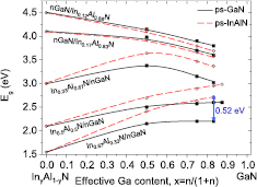
Figure 34. Calculated band gaps, Eg, for 1InyAl1−yN/nGaN and nGaN/1InyAl1−yN SLs in two different strain modes. Solid lines correspond to SLs in ps-GaN strain mode, dashed red lines correspond to SLs in ps-InAlN mode. The vertical blue arrow indicates the largest difference, ΔEg, between the two strain conditions. Reprinted figure with permission from [107], Copyright 2016 by the American Physical Society.
Download figure:
Standard image High-resolution imageWe can conclude that the influence of internal strain on band gap values in the 1InyAl1−yN/nGaN SLs with high In content is quite pronounced and similar like in 'binary' InN/GaN SLs (ΔEg around 0.5 eV). On the other hand it is much more significant than in GaN/AlN SLs (ΔEg below 0.05 eV).
6.2.2. Influence of electric field and wave function hybridization on the band gaps.
An internal electric field of 3.64 MV cm−1, due to spontaneous polarization, was reported as obtained from PL measurements performed on a set of nGaN/mIn0.18Al0.82N quantum structures [8].
The internal electric fields in wells of nGaN/mInyAl1−yN and mInyAl1−yN/nGaN SLs estimated from the semi-macroscopic model described in section 4.3.3, are illustrated in figures 35(a) and (b), respectively. The obtained electric fields are compared for selected SLs with the values calculated ab initio by the method described in section 4.3.2 (open circles in figure 35) and quite a good agreement is found, taking into account the model limitations. As it was already mentioned in section 4.3.3, the estimates from the model values of electric fields depend only on well to barrier thickness ratios (as follows from equations (1) and (2)), but not on the separate values of well and barrier thicknesses.
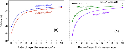
Figure 35. Electric fields in nGaN/mInyA1−yN (a) and mInyAl1−yN/nGaN (b) SLs as functions of well to barrier thickness ratio. In figure (b), the values estimated from the semi-macroscopic model (dots) are compared with the ab initio calculations (open circles). Lines are guides for the eyes.
Download figure:
Standard image High-resolution imageConsidering nGaN/mInyAl1−yN SLs (figure 35(a)), strong internal fields are found for very small values of well-barrier thickness ratios, whereas for higher ratios (above 4), they change rather slowly, approaching zero for the ratios above 10. A similar behavior of the electric field was observed in wells of mInyAl1−yN/nGaN SLs, with y = 0.67 and y = 0.50 (figure 33(b)). Comparing figures 33(a) and (b) we can conclude that the highest electric fields are obtained for SLs with highest In content, y (up to 9 MV cm−1 for y = 0.67) and weaker for SLs with smaller y values. An exception here is mIn0.33Al0.67N/nGaN SL where the electric field almost vanishes for all m/n values. It will be shown that this is due to the compensation of the spontaneous and the piezoelectric polarizations.
The semi-macroscopic model enables to analyze the electric fields in SLs in terms of contributions from the piezoelectric and spontaneous parts of polarization. The calculated spontaneous and piezoelectric components of polarization in nGaN/mInyAl1−yN and mInyAl1−yN/nGaN SLs, being differences in polarization between the InAlN and GaN layers, are shown in figure 36. We observe that both, spontaneous, Psp, and piezoelectric, Ppz, parts of the polarization depend almost linearly on In content, y. Around y = 0.17 (where well and barrier layers are lattice matched) the piezoelectric polarization vanishes, and only the spontaneous part contributes to the total polarization. The total polarization vanishes around y = 0.33, at the crossing of Psp and −Ppz lines, so the model confirms the finding that in mIn0.33Al0.67N/nGaN SLs the internal electric field is close to zero.
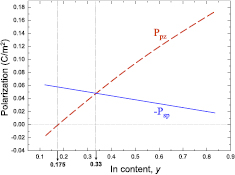
Figure 36. Spontaneous, Psp, and piezoelectric, Ppz, components of the total polarization in nGaN/In0.17Al0.83N and mInyAl1−yN/nGaN SLs. Reprinted figure with permission from [107], Copyright 2016 by the American Physical Society.
Download figure:
Standard image High-resolution imageSummarizing, SLs containing InyAl1−yN alloys can be analysed in three different regions of y values:
- 1.Low In content, y < 0.33Wells and barriers of the SLs are nearly lattice-matched. The internal strains are small and the electric fields are mostly due to the spontaneous polarization. Their influence on the band gaps is compensated to some extent by the hybridization of wave functions. At y ~ 0.17, the piezoelectric polarization vanishes due to the matching of GaN and InAlN lattice constants and the internal strain also vanish. The band gaps are similar to the gaps of the quaternary alloys with equivalent compositions.
- 2.y ~ 0.33The spontaneous and piezoelectric polarizations cancel and the built-in electric fields vanish. The band gap behavior is mostly due to other effects, as internal strain and hybridization of wave functions. The In0.33Al0.67N/1GaN SL represent somehow the border case between GaN/InyAly−1N and InyAly−1N/GaN SLs.
- 3.Large In content, y > 0.33Strong internal electric fields are observed in thin wells of the SLs with high In content (up to 9 MV cm−1 in In0.67Al0.33N/1GaN SL). It results in band gaps much lower compared to the gaps of InAlGaN alloy with the equivalent composition.
7. Comparison of nitride and oxide superlattices
Oxide and nitride semiconductors have many similar physical properties. In particular, concerning three binary nitrides, GaN, AlN, and InN with corresponding oxides, ZnO, MgO, and CdO, it is easy to realize similar lattice constants and band gaps, as it is shown schematically in figure 37. On the other hand, the ionicity of oxides is much larger than that characterizing nitrides. Moreover, in contrast to wide and successful applications of nitrides in optoelectronics and electronics, oxides are not used on such a large scale in the semiconductor industry. However, an increasing scientific interest in these latter semiconductors has been observed for the last two decades [109, 110].

Figure 37. Schematic Eg dependence of wurtzite nitride and oxide compounds on lattice constant, a. [114] John Wiley & Sons. © 2017 WILEY-VCH Verlag GmbH & Co. KGaA, Weinheim.
Download figure:
Standard image High-resolution imageTo illustrate the similarities and differences between the two groups of materials, we will compare the nitride alloys and SLs based on AlN and GaN with oxide structures based on ZnO and MgO. The main representatives of these groups of semiconductors, ZnO and GaN are formed from neighboring atoms in the Periodic Table (Z(Ga) = 31, Z(Zn) = 30, Z(N) = 7, Z(O) = 8) and have similar lattice parameters and similar direct energy gap, Eg, of 3.35 eV and 3.43 eV, respectively, and both crystallize in the wurtzite structure. However, ZnO has some advantages over GaN. The first one is characterized by much larger exciton binding energy in ZnO (Eex ≈ 60 meV) comparing to GaN (Eex ≈ 25 meV); consequently, it is expected that ZnO-based light emitters should be much brighter than GaN light emitters. The next advantage is that large bulk monocrystals of ZnO are easily available, suitable as cheap substrates for epitaxy.
Alloys and quantum structures are formed in the case of GaN by adding elements from Group III of the Periodic Table (Al or In), and in the case of ZnO by adding elements from group II (Mg, Cd or Be). In figure 37, a schematic illustration shows similar ranges of available band gap energies for nitrides and oxides, crystallizing in the wurtzite structure; however CdO and MgO are stable in the rocksalt phase and experimental data on their wurtzite phase are very scare [111].
7.1. GaAlN and ZnMgO alloys
Due to different MgO and ZnO crystallographic structures (rocksalt and wurtzite, respectively), MgxZn1−xO alloys have a tendency to be metastable. Phase segregation has been reported to occur in MgxZn1−xO for, x > 33%, with a maximum Eg of about 4.0 eV [112, 113]. It is interesting to observe that in MgxZn1−xO an increase of band gap with x is accompanied by a reduction of the lattice constant. This behavior is different from usually observed trends (see e.g. AlGaN case).
Our calculated band gaps for ZnxMg1−xO alloy in the wurtzite structure are compared in figure 38 with the band gaps obtained for GaxAl1−xN (see figure 2(b)), see also [114]. Additionally, our results for MgxZn1−xO are compared with the experimental data from the literature [112, 115–119] and a very good agreement is found.
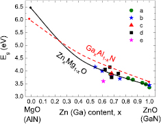
Figure 38. Band gaps of ZnxMg1−xO (solid black line) as a function of Zn-content in comparison with band gaps of GaxAl1−xN alloy (dashed red line). The lines represent fits to the calculated gap variations. Experimental data for ZnxMg1−xO are indicated, see: a = [112], b = [115], c = [116], d = [117], and e = [118]. [114] John Wiley & Sons. © 2017 WILEY-VCH Verlag GmbH & Co. KGaA, Weinheim.
Download figure:
Standard image High-resolution imageIn both alloys we observe similar Eg dependence on composition, but different composition dependent band gap bowings, b(x), which are defined through equation (2). In a linear approximation: b(x) = α + βx.
The band gap bowing of GaxAl1−xN alloy is small, b = 0.71 eV for x = 0.5 (α = 0.75, β = −0.07), which likely results from almost the same covalent radii, 1.22 Å for Ga and 1.21 Å for Al and similar lattice parameters.
The calculated bowing parameter of ZnxMg1−xO is larger, and with increasing Zn content, x, changes from 1 to 3 eV, being equal to 2.6 eV for x = 0.5 (α = 0.8, β = 3.4). Larger is also the difference in size of the cations. The covalent radius for Zn is equal to 1.22 Å and is 1.41 Å for Mg. In this respect, we can compare ZnxMg1−xO to InxGa1−xN where Eg bowing is also quite large and similar as in ZnxMg1−xO, ranging from 1.4 to 2.8 eV. Covalent radii of the cations are equal to 1.22 Å for Ga and 1.42 Å for In, the values are almost the same as for Zn and Mg, respectively.
Considering the band gap bowing in ZnxMg1−xO, an involvement of other factors should be also taken into account. We will mention here a very small value of c/a in MgO (1.55) and the high iconicity of this material resulting in a tendency to crystalize in rocksalt structure. All the above results in a large displacement of atoms by alloying. The above finding differ from the one obtained by Toporkov et al [115] where the Eg bowing for the ZnxMg1−xO alloy was found to be very small (b = 0.237 eV). The experimental MgxZn1−xO bowing parameter is unknown due to a limited range of available compositions (up to 40% of Mg), but the good agreement with the calculated band gaps (figure 38) indicates that the experimental Eg bowing should likely be also large.
7.2. GaN/AlN and ZnO/MgO SLs
To compare the short period SLs of the form: mGaN/nAlN and mZnO/nMgO, we choose the most typical growth direction along the wurtzite c-axis. Such a comparison is interesting because not only QWs (GaN and ZnO), but also QBs (AlN and MgO) are similar (Z(Al) = 13, Z(Mg) = 12).
In figure 39, energy band gaps versus number of barrier MLs, n, are presented for mZnO/nMgO (a) and mGaN/nAlN (b) SLs. Comparing figures 39(a) and (b), we observe surprisingly similar Eg behavior in both kinds of SLs. The range of the Eg variation is almost the same, and they exhibit the same trends with changing m and n. In both cases, with an increasing number of QW layers, m, Eg is significantly reduced. On the contrary, increasing the barrier width, i.e. n, leads to increase (smaller m) or decrease (larger m) of Eg.

Figure 39. Band gaps of mZnO/nMgO (a) and mGaN/nAlN (b) SLs as functions of the number of barrier MLs, n.
Download figure:
Standard image High-resolution imageAnalysing the contributions to the band gap evolution, we can estimate the influence of the internal strain as not substantial, due to similar lattice constants of quantum layers and substrates (GaN in mGaN/nAlN and ZnO in mZnO/nMgO). The interplay of the built-in electric field and wave functions hybridization should mostly influence the Eg behavior. The effect of the internal electric field will be discussed in the next section.
7.3. Internal electric field
The electric fields in the wells (Ew) and barriers (EB) of the mZnO/nMgO SL structures are estimated from the semi-macroscopic model described in section 4.3.3 and presented in figure 40. The values of the parameters for ZnO and MgO used in the model calculations are listed in table 4. Note that lattice matching to ZnO substrate is assumed.
Table 4. Lattice constants a (Å), ML thicknesses lw,b (Å), spontaneous polarizations Psp (C m−2), piezoelectric coefficients, elastic constants, and dielectric constants, χ, used in the calculations of the electric fields.
| ZnO | MgO | |
|---|---|---|
| A | 3.198 | 3.228 |
| lw,b | 2.578 | 2.500 |
| Psp | −0.053 [120] | −0.080 [120] |
| e31 | −0.55 [120] | −0.78 [120] |
| e33 | 1.24 [120] | 0.14 [119] |
| c13 | 84 [120] | 88 [120] |
| c33 | 176 [120] | 222 [120] |
| χ | 7.4 [121] | 9.8 [121] |
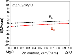
Figure 40. Internal electric fields in wells (Ew) and barriers (Eb) of mZnO/nMgO SLs as functions of the effective Zn content. [114] John Wiley & Sons. © 2017 WILEY-VCH Verlag GmbH & Co. KGaA, Weinheim.
Download figure:
Standard image High-resolution image
Figure 40 illustrates the internal electric fields in wells (Ew) and barriers (EB) of mZnO/nMgO SLs as functions of the effective Zn content x. One can see that the built-in electric field in ZnO/MgO is weak, approaching 2 MV cm−1. Comparing with mGaN/nAlN SLs (figure 11(b)), we observe a big difference in the electric fields strengths. The built-in electric field in mGaN/nAlN is strong, reaching 12 MV cm−1. The above difference could be explained by the analysis of the spontaneous and piezoelectric contributions to the polarization. In mGaN/nAlN the signs of spontaneous and piezoelectric polarizations are the same (a(GaNsubstrate) > a(AlNbarrier)), contrary to the case of mZnO/nMgO where spontaneous and piezoelectric parts have opposite signs (a(ZnOsubstrate) < a(MgObarrier)), partially compensating, to result in a small total polarization and low strenght of the electric field.
In conclusion, comparing GaN–AlN and ZnO–MgO systems, we found many similarities, but also some differences. We found very similar behavior of the band gaps in GaxAl1−xN and ZnxMg1−xO alloys; they cover almost the same range of values and exhibit similar trends, but there are substantial differences in the band gap bowings. Comparing mGaN/nAlN and mZnO/nMgO SLs, we observe a similar evolution of the band gaps with varying number of atomic MLs, whereas the strengths of the built-in electric fields, existing in these two families of SLs differ significantly.
8. Summary and outlook
In summary, a study of the band gap engineering in short period nitride SLs based on first principles calculations was presented. All the factors influencing the band gap behaviour were analysed and discussed.
The evolution of the band gaps and electric fields was illustrated and discussed using two ways of presentation. The first one consists of dependences on effective cation concentration. Such a choice was motivated by the concept of comparison with corresponding alloys. The second way uses the numbers of barrier and well monolayers. The latter approach is based on more intuitive understanding and enables to expose new microscopic mechanisms leading to SL formation (discussion of the wave functions overlaps and oscillator strength).
It was shown that, for superlattices, it is possible to exceed by far the range of band gap values which can be realized in ternary alloys. By comparing band gaps in SLs grown along different directions of the wurtzite structure, or with different atomic arrangements, we demonstrated the effects of lattice geometry. To evaluate the effect of internal strain, two cases of growth conditions were compared: the pseudomorphic and free-standing. It was shown, assuming a given growth orientation and strain conditions, that the band gaps are influenced mainly by the built-in electric field, Eel (in polar structures) and by the wave function hybridization. The contributions of these two important factors to the band gap behavior are illustrated and estimated quantitatively. It appears that there are two interesting ranges of layer thicknesses; in one (few MLs in barriers and wells) the influence of the wave function hybridization is dominant, whereas in the other (layers thicker than roughly 5–6 MLs) the effect of the internal electric field is more important.
Finally, to show the specifics of nitride structures, a comparison of GaN/AlN and ZnO/MgO SLs was performed, pointing out the similarities and differences between nitride and oxide SLs. Comparing GaN/AlN and ZnO/MgO SLs, we found a large difference in the internal electric field strengths. In light of the above findings, it is very surprising that the band gaps of ZnO/MgO and GaN/AlN SLs are so similar, covering the same range of values and exhibiting the same trends. Additionally, we found substantial differences in GaxAl1−xN and ZnxMg1−xO band gap bowings.
The obtained results provide insight in the properties of nitride SLs with relevance to band gap engineering and consequently to device optimization. The idea of short period SLs is very complex and crucial to understand in detail for the realization in optoelectronics based on nitride quantum structures. Many problems remain to be solved. It is important to comment on the availability of real structures. Up to now the most popular crystal growth orientation was the polar one, but we observed increasing interest, within the nitride community, in the properties of semipolar and nonpolar structures including, both, theoretical and experimental investigations. It is quite challenging to obtain binary mInN/nGaN SLs. Instead of intentionally introduced InN QWs, InxGa1−xN layers are grown in such structures. Using both growth methods metalorganic vapour phase epitaxy or molecular beam epitaxy, produce InxGa1−xN/GaN structures with x not higher than 0.3–0.4. Low In incorporation may be a general property for all SL samples presented so far.
Concerning the comparison of the measured band gaps in such mInxGa1−xN/nGaN SLs (x ⩽ 0.35) with theoretical predictions, demonstrated in this work, the agreement is satisfactory. Moreover, measured hydrostatic pressure dependence of Eg in different samples goes along with the theoretical calculations. It represents a strong experimental verification of the used approach and strongly suggests much lower In-concentration in quantum wells of considered SLs than the intended ones. Another interesting issue is the ordering of In cations in ultrathin InGaN layers. Preferential concentrations of x = 0.33 and 0.66 has been considered by Limperakis et al [106].
Below we present a partial list of issues which are important for understanding properties of In(Ga)N/GaN SLs, i.e. structures which demonstrate anomalies in both their growth parameters and physical mechanisms of band structure, lattice vibrations, heat transport, and doping. Developing a controllable growth processes of InxGa1−xN/GaN short period superlattice will lead to:
- (a)a solution to limitations in obtaining high In-content quantum structures and devices based on InGaN QWs that operate in amber, red and infrared spectral regions;
- (b)a description of atoms arrangement in alloys for the case of ions with significantly different size and chemical bond strength (e.g. In versus Ga and In–N versus Ga–N, correspondingly), in particular ordering of cations, and its relation to growth conditions;
- (c)the experimental verification of SPSLs properties grown on N-side of GaN substrate or InGaN pseudo-substrate;
- (d)
Acknowledgments
This work was partially supported by the Polish National Science Center, grants DEC-2013/11/B/ST3/04263 and DEC-2014/15/B/ST3/04105.