
Abstract
A coupled two-temperature, molecular dynamics methodology is used to simulate the structural evolution of bcc metals (Fe and W) and fcc metals (Cu and Ni) following irradiation by swift heavy ions. Electronic temperature dependent electronic specific heat capacities and electron–phonon coupling strengths are used to capture the full effects of the variation in the electronic density of states. Tungsten is found to be significantly more resistant to damage than iron, due both to the higher melting temperature and the higher thermal conductivity. Very interesting defect structures, quite different from defects formed in cascades, are found to be created by swift heavy ion irradiation in the bcc metals. Isolated vacancies form a halo around elongated interstitial dislocation loops that are oriented along the ion path. Such configurations are formed by rapid recrystallization of the molten cylindrical region that is created by the energetic ion. Vacancies are created at the recrystallization front, resulting in excess atoms at the core which form interstitial dislocation loops on completion of crystallization. These unique defect structures could, potentially, be used to create metal films with superior mechanical properties and interesting nanostructures.
Export citation and abstract BibTeX RIS

Original content from this work may be used under the terms of the Creative Commons Attribution 3.0 licence. Any further distribution of this work must maintain attribution to the author(s) and the title of the work, journal citation and DOI.
1. Introduction
The modification of materials by ion and laser irradiation has the potential to introduce novel nanostructures and properties not achievable by any other material processing methods. In particular, very energetic ions can induce elongated features with nanometre width and micron depth, usually referred to as ion tracks, that have properties quite distinct from the bulk material. Since their observation in lithium flouride [1] in 1958, ion tracks have been observed in many other insulators [2–5], semi-conductors [6–12], and even amorphous semi-conductors [13]. Various metals [14–17] have also been irradiated with swift heavy ions, however, the damage observed is distinct from that of band gap materials. Metals show a remarkable resistance to ion track formation, with damage (if any) taking the form of small defect clusters.
Material modification via swift heavy ion irradiation (SHI) is already used in a range of industrial processes, including the generation of nanopores in polymers [18, 19], allowing controlled drug delivery in biomedicine [20], or the filtration of bacteria from water. Swift heavy ion irradiation has also been used for the fabrication of quantum devices [21–23] and they are widely used to generate novel metal silicides via ion beam mixing [24], which are formed at the interface of integrated circuit technologies. Swift heavy ions may prove important in the generation of high temperature superconductors, as ion tracks in Bi2Sr2CaCu2O8+x provide efficient pinning sites [25], significantly enhancing the critical superconducting current of the material at higher temperatures.
Energetic ions moving through solids dissipate their energy by elastic collisions with target nuclei, displacing them from their equilibrium positions. In addition, they lose energy by inelastic collisions with electrons, resulting in electronically excited regions in the solid. The energy loss per unit distance of an ion moving in a solid is referred to as the stopping power. The energy loss by elastic collisions with nuclei is known as the nuclear stopping power and the energy loss by inelastic collisions with electrons is known as the electronic stopping power. The ratio of the nuclear stopping power to the electronic stopping power, that is the relative proportion of energy dissipated by these two mechanisms, depends on the energy of the impinging ion. For very energetic ions, known as swift heavy ions, the interaction cross section of the nuclei is extremely low, therefore energy dissipation is primarily by electronic excitations. The passage of such ions results in a cylindrical track of highly excited electrons, which, over time, relax to the ground state and transfer some or all of their energy to the atoms, resulting in lattice heating and, in some cases, the formation of ion tracks.
The sensitivity of a material to ion track formation following SHI irradiation varies broadly, with some experiencing damage with electronic stopping powers as low as 2 keV nm−1 [26], while others appear to be undamaged for stopping powers as high as 86 keV nm−1 [14]. Insulators such as SiO2 and Y3Fe5O12 are particularly sensitive to damage [27] whereas metals appear to be relatively insensitive [14]. This resistance to damage of metallic materials is attributed to the high mobility of the electrons in the metal, resulting in energy transport away from the track before energy can be transfered to the atoms. There has, therefore, been much less interest in swift heavy ion irradiation in metals than in insulators. Nevertheless, SHI damage has been detected in Fe and in W [14, 16]. Indeed, interesting defect structures that were attributed to dislocation lines oriented along the path of the ion track were observed in Fe using TEM [14]. Such an effect warrants further investigation, as the ability to create dislocations in a controllable manner in nanoscale metal films has a range of potential applications in nanotechnology. W is a candidate plasma facing material in future fusion reactors, so a thorough understanding of how it reacts in radiation hard environments is important for the nuclear industry.
Swift heavy ion irradiation is generally modelled using the two-temperature model [28] (based on the earlier inelastic thermal spike model [29]), which solves two coupled thermal diffusion equations, one for the electronic temperature and one for the lattice temperature, in cylindrical coordinates. Energy is deposited initially in the electronic system, centred on the origin of the cylindrical cell, and this energy diffuses radially while simultaneously transferring to the lattice via electron–phonon coupling. Above a certain threshold stopping power, the temperature in a cylindrical region exceeds the melting temperature and the diameter of the resulting ion track is assumed to be equivalent to the diameter of the molten region.
This two-temperature model has been used successfully to explain many of the observed phenomena. However, there are a number of severe approximations which make it challenging to obtain quantitative predictions. In particular, superheating and recrystallization are not accounted for in the model and these effects invalidate the one to one correspondence between the radii of the molten region and the ion track. Coupling the two temperature model with molecular dynamics (2T-MD) addresses some of these issues [30]. In this paper we employ 2T-MD to model the effects SHI irradiation in Fe, W, Cu, and Ni as a function of stopping power. We find that, for the bcc metals, in contrast to the commonly held belief that metals are insensitive to such irradiation, interesting defect structures are created along the ion path, which bear a striking resemblance to the defects observed by TEM two decades ago.
2. Methodology
2.1. Two temperature molecular dynamics
We employ the two temperature molecular dynamics (2T-MD) model described in [30], implemented in DL_POLY_4 [31], and used previously for modelling for SHI irradiation in metals [32, 33] and semiconductors [34, 35]. In this model the electronic temperature (Te) evolution is described by a thermal diffusion equation,
with Te dependent electronic specific heat capacity,  , and electron–phonon coupling parameter,
  . The electronic thermal conductivity,
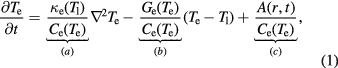
  , is assumed to depend only on the lattice temperature (Tl) and to be spatially independent. The first term on the right hand side of equation (1), (a), represents electronic heat diffusion and the second term, (b), represents energy exchange with the lattice via electron–phonon coupling. The third term, (c), is a source term representing the energy deposited in the electronic system by the SHI, at a distance r from the ion path at time t. We assume that the SHI travels normally (z) through the material and that the energy deposition is independent of z. A(r,t), has a Gaussian spatial dependence and an exponentially decaying time variation;

Here α equals  where τ is the characteristic temporal deposition time (assumed to be 1 fs) and D(r) is a Gaussian function describing the spatial variation of the energy deposition.
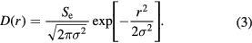
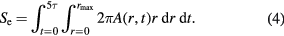
Here r is the lateral distance from the centre of the projectile's path and σ is the standard deviation of the Gaussian spatial deposition, equal to 1 nm in our simulations. A is a normalization constant that ensures that the spatial and temporal integration equates to the energy deposited into the electronic system (the electronic stopping power, Se, of the swift heavy ion [36]).
In this study we have considered stopping powers ranging from 10 keV nm−1 to 100 keV nm−1, with increments of 10 keV nm−1.
The structural evolution of the lattice is calculated using molecular dynamics (MD) and the energy exchange with the electronic system in equation (1) is included via a Langevin thermostat, with the local electronic temperature (Te) used as the thermostatting temperature [30].The MD equation of motion for an atom with mass m is given by;
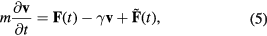
where  is velocity of the atom at time t,
  is the deterministic force due to the interatomic potential,
  is the frictional force (with friction coefficient γ) that represents energy loss due to electronic drag and
  is a stochastic force which is thermostatted at the electronic temperature. Thus energy lost/gained from the (b) term in equation (1) is gained/lost by the MD cell. Equation (1) is solved numerically by dividing the simulation cell into voxels and using a variable time step finite difference solver. The centre of the cell overlaps with the MD simulation cell to allow energy exchange between the two sub-systems (figure 1). The electronic simulation cell extends well beyond the atomistic simulation cell to enable energy to be transported away from the atomistic cell by electronic thermal conduction. The MD simulation cell has periodic boundary conditions in all 3 directions. For the electronic simulation cell we use von Neumann (zero flux) boundary conditions with zero normal derivative in the z direction to impose zero electronic heat flux in this direction. In the perpendicular (x,y) directions we aim to simulate heat transport through the bulk material beyond the electronic simulation cell, therefore we impose Robin (variable flux) boundary conditions to the electronic cells in the x,y directions. The Robin boundary conditions are a weighted combination of Dirichlet (infinite flux) and von Neumann boundary conditions and they provide a method for gradually dissipating electronic energy from the boundaries of the cell to simulate electronic thermal conductivity through the bulk. In our case we take
  to be
to be  on the cell boundaries in the x and y directions to simulate electronic energy dissipation by conduction through the bulk.

Figure 1. Schematic representation of the 2T-MD methodology. Energy is deposited into the electronic system in the central region. The electronic temperature voxels extend beyond the MD simulation cell.
Download figure:
Standard image High-resolution image2.2. MD simulation details
The MD simulations cells for Fe and W have  cubic unit cells (2350000 atoms). The simulation cell was subdivided into
  coarse-grained cells for Fe (
 for W). These coarse grained cells overlap with the voxels of the electronic system to enable energy exchange. The electronic system had
  voxels for Fe and
  for W, to extend beyond the boundaries of the MD cell in the x and y directions (figure 1). The fcc MD simulation cells have 2420000 atoms (
 cubic unit cells). The extended Finnis Sinclair interatomic potentials [37] were used for all metals and the simulation cell was equilibrated for 200 ps at 300 K and 1 atmosphere, using the Nosé Hoover thermostat and barostat, prior to initiating the SHI simulations by energy deposition to the electronic system. A time step of 1 fs was used for all MD simulations.
2.3. Electronic thermal parameters
The temperature dependent electronic specific heat capacity,  , and electron–phonon coupling
  for all the metals (Fe, W, Cu and Ni) were calculated by Lin et al [38] using density functional theory. The
  used for W was modified slightly, based on the recent measurement of the ground state value [39]. The full Te variation for W, and a comparison with [38], is shown in [40]. The electronic thermal conductivities were assumed to depend only on the lattice temperature and the temperature dependence was taken from Kaye and Laby [41].
3. Results and discussion
3.1. Temperature evolution
The time evolution of the local lattice and electronic temperatures at the centre of the simulation cells during a 60 keV nm−1 SHI irradiation is shown in figure 2. Fe has a higher electronic specific heat capacity at high Te than W, therefore the peak electronic temperature is lower (due to (c) in equation (1)). However, the higher electron–phonon coupling strength of W results in a higher rate of energy exchange with the lattice, causing the lattice temperature of W to increase more rapidly than Fe. The electronic and lattice temperatures equalise at around 2 ps in Fe and relax to ambient temperatures at the same rate. In W the electronic temperature falls below the lattice temperature, with energy subsequently flowing from the lattice to the electrons. Both systems reach ambient temperatures after approximately 80 ps.

Figure 2. Evolution of the electronic and lattice temperatures at the centre of Fe (red lines) and W (blue lines) simulation cells following irradiation by a 60 keV nm−1 SHI. The electronic temperatures are denoted by dashed lines, and the lattice temperatures by solid lines.
Download figure:
Standard image High-resolution imageThe temperatures at the central region of the cells highlight how the peak temperatures evolve, however, greater understanding of the structural evolution is obtained from the temperature evolution of a cross section of the simulation cell, as shown in figure 3. Significant differences are observed between the time evolution of Te for W and Fe. In both cases the initial electronic temperature rises in the centre of the simulation cell and spreads via diffusion and, simultaneously, energy transfers to the lattice via electron–phonon coupling. The most striking difference observed is due to the significantly higher electronic diffusivity of W. As a result of the high diffusivity, energy rapidly diffuses to the edges of the cell, resulting in a lower Te at the centre of the cell for W than for Fe. Interestingly, despite these extreme differences in the electronic temperature profiles, the corresponding lattice temperature cross-sections, shown in figure 4, are remarkably similar. This is due to a combination of the differences in the thermal properties of the lattice and the electron–phonon coupling strength.

Figure 3. Cross-section of electronic temperatures in Fe (a) and W (b) at various times following a 60 keV nm−1 SHI irradiation event.
Download figure:
Standard image High-resolution image
Figure 4. Cross-section of lattice temperatures in Fe (a) and W (b) at various times following a 60 keV nm−1 SHI event. The dashed horizontal line illustrates the melting temperature of each respective interatomic potential.
Download figure:
Standard image High-resolution imageThe melting temperature is a key property for resistance to damage by SHI irradiation. The lower melting temperature of Fe means that, despite similar lattice temperature profiles, a much wider region of the cell exceeds the melting temperature for Fe than for W, and the melting temperature is exceeded for a longer period of time. At 5 ps there is a cylindrical region of about 30 nm diameter in the Fe cell that is above the melting temperature and the corresponding diameter in the W cell is only 5 nm. Thus, it is expected that W will be significantly more resistant to SHI radiation damage than Fe.
3.2. Defect evolution
A view along the [100] direction of the simulation cell of Fe, at various times following a 60 keV nm−1 SHI irradiation event, is illustrated in figure 5. The figure shows both the time evolution of the Wigner–Seitz (WS) defects (left-hand column) and the evolution of the amorphised volume and dislocations (right-hand column). The Wigner–Seitz defects were calculated using Voronoi cell analysis [42] in OVITO [43]. The dislocations were also detected using OVITO [44]. 10 ps after irradiation a large amorphous or molten region is established at the centre of the simulation cell. As the simulation proceeds, and the lattice temperature cools, the metal starts to recrystallize and a cylindrical recrystallization front shrinks the molten region. The rapid recrystallization leaves a number of isolated vacancies in its wake, and a much lower number of interstitials. The excess of vacancies produced results in an excess of atoms at the centre of the cell, after complete recrystallization. The excess atoms create interstitials, which cluster and collapse to form dislocation loops that are aligned approximately parallel to the direction of the ion path. Two types of loops are formed, one type has Burgers vectors  and the second type have
  Burgers vectors, which generally have higher energies than
  loops in bcc metals. The total length of dislocations with
  is 336 Å, and for
  this length is 106 Å.
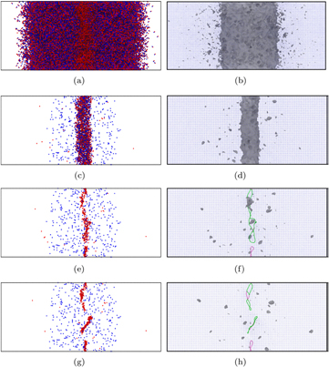
Figure 5. Side profile of defect evolution in Fe during a 60 keV nm−1 simulation. The left column illustrates Wigner–Seitz defect evolution, with red dots representing interstitials and blue dots representing vacancies. The right column shows dislocation loop creation (the green lines are  and the purple are
  ). The dark grey regions are regions which deviate from the perfect lattice. (a) 10 ps. (b) 10 ps. (c) 30 ps. (d) 30 ps. (e) 50 ps. (f) 50 ps. (g) 150 ps. (h) 150 ps.
Download figure:
Standard image High-resolution imageWe note that this defect configuration, with a halo of vacancies surrounding aligned dislocation loops, is quite distinct from that observed in cascade simulations that model low to moderate ion irradiation. In cascades, vacancies tend to reside near the ion path and dislocation loops migrate further from the path. In contrast to cascade simulations, the cross-section for nuclei interactions is extremely low at the stopping powers considered here so there are no knock-on atoms in our simulations. The residual defects are all created by the recrystallization of the molten region. Vacancies are created at the recrystallization front and these vacancies are immobile due to the high activation energy for migration. As the cylindrical molten region shrinks, there is an excess of atoms and these atoms, necessarily, form interstitials close to the ion path. For sufficiently high interstitial densities, these interstitials cluster to form pure edge (prismatic) dislocation loops. The conformation of the dislocations bear a striking resemblance to TEM characterization of polycrystalline Fe irradiated with C60 fullerenes [14], where 'two quasi-parallel dislocation lines joined near the surface' were observed. Experiments involving cascade damage in Fe [45] also create  and
and  interstitial dislocation loops but in these cases the loops are not elongated and they are oriented in random directions.
W shows much less damage than Fe, due to the combination of higher diffusivity and higher melting temperature. The morphology of the defects created by a 60 keV nm−1 ion is shown in figures 6(a) and (b). It is clear, by comparison with figure 5, that a lower number of defects was formed but that they show the same features as Fe, namely that there is a residual halo of isolated vacancies surrounding interstitial dislocation loops, which is further confirmed by the defect distribution plot shown in figure 7. The time evolution of the number of Wigner–Seitz defects is plotted for Fe and W in figure 8, which clearly shows the reduced damage in W.

Figure 6. The final defect distribution in W following a 60 keV nm−1 SHI simulation. (a) illustrates Wigner–Seitz defect evolution, with red dots representing interstitials and blue dots representing vacancies. (b) shows dislocation loop creation (the green lines are  , and purple lines are
  ). The dark grey regions are regions which deviate from the perfect lattice. (a) 80 ps WS image. (b) 80 ps dislocation image.
Download figure:
Standard image High-resolution image
Figure 7. Histogram of the final number of vacancies (purple) and interstitials (orange) as a function of radial distance from the ion path for a 150 ps 60 keV nm−1 W simulation.
Download figure:
Standard image High-resolution image
Figure 8. The time evolution of the number of WS defects in Fe and W for 60 keV nm−1 SHI simulations.
Download figure:
Standard image High-resolution imageSHI irradiation experiments done on W [15] did not find any evidence of defect creation up to stopping powers of 70 keV nm−1, however, these experiments were performed at low temperatures (25 K). At these temperatures the thermal conductivity of W is significantly enhanced over the room temperature value (2320 W m−1 K−1 [46] compared to 177 W m−1 K−1 at room temperature), which dissipates the deposited energy before energy transfer to the lattice. We repeated our simulations at 25 K, using the appropriate value for the thermal conductivity, and found no residual defects at an electronic stopping power of 70 keV nm−1.
The number of Wigner–Seitz defects created in Fe and W as a function of stopping power is presented in figure 9. Such plots give an indication of the threshold stopping power, i.e. the stopping power below which no residual damage is created. For Fe the threshold is estimated to be 10 keV nm−1 and for W the higher threshold of 30 keV nm−1 is observed. The number of defects is observed to increase approximately linearly with stopping power. The variation in the length of residual dislocation lines is plotted in figures 9(b) and (c). It is clear that  dislocations dominate over
  dislocations and there is a general trend of increasing dislocation line length with stopping power. A decrease in length of
  generally corresponds to an increase in the length
  dislocations. Further investigation revealed that
  dislocations were created by the overlap of two
  loops, as previously observed in cascade simulations [47].

Figure 9. Defect creation in Fe and W as a function of Se. (a) shows the number of WS defects as a function of Se. (b) shows the length of dislocation loops found in Fe as a function of Se. (c) shows the length of dislocation loops found in W as a function of Se. The total dislocation loop length increases with stopping power, but there is a more complex interdependence on the evolution of each type of dislocation loop.
Download figure:
Standard image High-resolution image3.3. Face centred cubic metals
A similar investigation was performed for the fcc metals, Cu and Ni. As expected from earlier experiments [14, 15], these metals proved to be very resistant to damage, with no residual defects being observed up to stopping powers of 60 keV nm−1 in Ni and a very small number (32) of defects in Cu at this stopping power. However the reason for the resistance to damage was different for the two metals. In Cu it is due to the high electronic thermal conductivity, which enables energy to diffuse rapidly away from the ion path. The rapid diffusion of electronic energy ensures that energy is transported away from the track before the electron–phonon coupling has time to transfer a significant amount of energy to the lattice and melting is limited. In Ni, however, it is the decrease in the electron–phonon coupling strength with increasing electronic temperature that is primarily responsible for decreased energy transfer to the lattice. The electronic temperature dependence of the electron–phonon coupling constant for Cu and Ni [38] is shown in figure 10, which illustrates the very low coupling for Ni at high Te. The lattice temperature evolutions for 60 keV nm−1 simulations for Cu and Ni are shown in figure 11. There is no detectable rise in lattice temperature for Ni due to the weak electron–phonon coupling at high electronic temperatures. The lattice temperature of Cu rises above the melting temperature in a narrow region (radius 4 nm) and results in limited melting and the creation a small number of defects. As with Fe and W, the vacancies are isolated and the interstitials form very small clusters. These results highlight that the electronic temperature dependence of the material parameters (electronic diffusivity and electron–phonon coupling) can play a crucial role in the resistance of metals to damage by SHI irradiation.

Figure 10. The electron–phonon coupling contsant as a function of Te for Cu and Ni. Data taken from [38].
Download figure:
Standard image High-resolution image
Figure 11. Cross-section of lattice temperatures in Ni (a) and Cu (b) at various times following a 60 keV nm−1 SHI irradiation event. The dashed lines show the melting temperatures for the interatomic potentials employed in the simulations.
Download figure:
Standard image High-resolution image
4. Conclusions
A series of 2T-MD simulations was carried out to model the structural evolution of Fe and W following swift heavy ion irradiation. It was found that W was more resistant to damage than Fe, primarily due to its higher melting temperature, and that above the threshold stopping power 10 keV nm−1 for Fe and 30 keV nm−1 for (W) the number of defects increased linearly with stopping power. Interesting defect structures were created that were very different to those observed in cascade simulations that model the effects of lower energy ion irradiation. In the SHI simulations, a halo of isolated vacancies were formed within a few nm of the ion path and interstitial clusters were concentrated very close to the path. These clusters took the form of dislocation loops with predominantly  Burgers vectors, along with some loops with
  character. The
  loops appeared to be formed by overlap between two
  loops. The dislocation loops were highly elongated and they were aligned roughly parallel to the ion path, closely matching a description of SHI damage in Fe imaged by TEM in Fe [14].
The location of the interstitial clusters close to the ion path, and the isolated vacancies further from the path, can be explained by the cylindrical recrystallization front. Energy deposited to the lattice from the excited electrons along the ion path results in a cylindrical volume of molten metal. As energy diffuses away, and the lattice cools, recrystallization occurs at the surface of the cylinder. The rapid crystallization results in the formation of quenched-in vacancies. As the recrystallization front approaches the centre of the path, there is an excess of atoms, due to the quenched-in vacancies, and these necessarily form interstitials in the recrystallized lattice. The high mobility of interstitials in bcc metals result in clustering and the formation of low energy dislocation loops, as observed in the simulations. Such dislocation loops should be a general feature of SHI irradiation in metals that are sensitive to damage.
Two fcc metals, Ni and Cu, were also investigated, but no residual damage was found in Ni up to 60 keV nm−1 and only a very small number of defects in Cu. The resistance to damage is due to the high thermal conductivity in Cu, however, in Ni it is the strong decrease in the electron–phonon coupling at high electronic temperature that is the primary reason for the reduced damage. A number of material parameters (melting temperature, electronic thermal conductivity and electron–phonon coupling strength), and their electronic temperature dependence, have a strong influence on the resistance of metals to damge induced by SHI irradiation. The high thermal conductivity and relatively low electron–phonon coupling of fcc metals render them relatively insensitive to damage, in spite of their relatively low melting temperatures. The strong electron–phonon coupling of the bcc metals (Fe and W) is primarily responsible for the sensitivity of these metals to damage.
In summary, SHI irradiation of Fe and W was found to create elongated dislocation loops that were oriented along the ion path. The results imply that irradiating metal films with energetic ions is a potential method for controlling the microstructure to increase the tensile strength. There is also the potential for taking advantage of pipe diffusion along dislocation cores to create a controlled spatial variation of dopants in metal films.
Acknowledgments
GSK acknowledges funding from the European Office of Aerospace Research and Development, STM acknowledges funding from the Leverhulme trust (grant number RPG-2013-331). Via our membership of the UKs HPC Materials Chemistry Consortium, which is funded by EPSRC (EP/L000202), this work made use of the facilities of ARCHER, the UKs national high-performance computing service, which is funded by the Office of Science and Technology through EPSRCs High End Computing Programme. Additional computational resources were provided by the high performance computer cluster GRACE at UCL.