

Abstract
Magnetoresistive (MR) sensors have been successfully applied in many technologies, in particular readout electronics and smart systems for multiple signal addressing and readout. When single sensors are used, the requirements relate to spatial resolution and localized field sources. The integration of MR sensors in adaptable media (e.g. flexible, stretchable substrates) offers the possibility to merge the magnetic detection with mechanical functionalities. In addition, the precision of a micrometric needle can benefit greatly from the integration of MR sensors with submicrometric resolution. In this paper, we demonstrate through several detailed examples how advanced MR sensors can be integrated with the systems described above, and also with microfluidic technologies. Here, the challenges of handling liquids over a chip combine with those for miniaturization of microelectronics for MR readout. However, when these are overcome, the result is an integrated system with added functionalities, capable of answering the demand in biomedicine and biochemistry for lab-on-a-chip devices.
Export citation and abstract BibTeX RIS
1. Introduction
Current demands for affordable integrated healthcare systems providing monitoring, diagnosis and therapy are leading to an increase in the development of integrated systems for lab-on-a-chip (LOC) devices. These platforms have the ability to identify biochemical products, toxins or disease symptoms, and allow biological screening assays or targeted drug delivery [1–3]. Hence, one finds enormous pressure to combine distinct functionalities and technologies for sensing and actuation, while resorting to low-cost fabrication methods that allow high throughput and wafer-level integration, enabling a straightforward transfer for high-volume industrial production settings [4].
Microfluidics is the core technology for LOC devices [5], providing reliable handling, manipulation and analysis of minute sample quantities with high-output sampling capabilities. Microfluidic-based platforms, in particular polymer-based microfluidics, stand out as a good example of portable instrumentation with the potential to combine affordable fabrication and versatile structuring. The common approach for integrating functional structures with microfluidic channels relies on patterning microdevices via Si-based semiconductor processes (e.g. lithography, deposition, etching) and bonding the chip to a pre-formed polymer microfluidic network (e.g. via ozone plasma, corona) [3, 6].
Smart systems integration of multiple technologies provides added functionalities such as sensing, actuation, signal processing or communication with applications in several sectors from healthcare to energy-efficient systems. The ability to match distinct technologies is a growing and not much explored route to provide ultra-compact heterogeneous integration of hybrid systems within multifunctional chips.
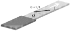
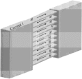
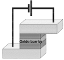
In this paper we describe different methodologies for microfluidic channel integration with magnetic devices used in magnetoresistive (MR) sensor technologies (figure 1). The choice of MR sensors results from their outstanding achievements in many areas, from reading magnetic bits for information storage (magnetic hard disk recording) to nanoparticle detection in biomedical platforms or neuronal synaptic activity measurements in neurosciences. Irrespective of the application, the integration of MR sensors offers quantitative functionality to biosensing (e.g. comparing to optical or chemical methods), while bringing new challenges to the design and fabrication of a solid-state device.
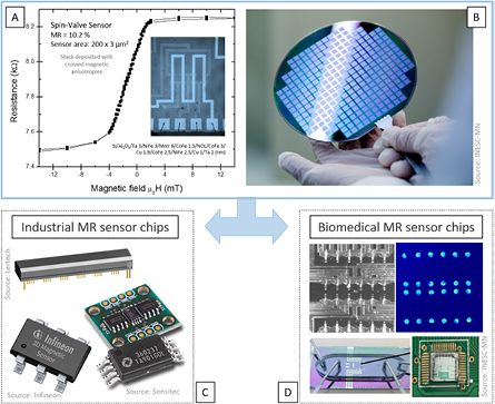
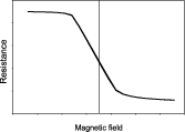
Figure 1. (A) and (B) MR sensor characteristic curve for a microfabricated structure. Low-cost and large-scale production compatible with semiconductor electronics fabrication at wafer level. (C) Examples of packaging of commercial MR chips where the sensor surface is hidden inside the case. (D) Examples of INESC-MN custom-made MR biochips where the sensor surface is accessible for biological/liquid sample contact.
Download figure:
Standard image High-resolution image2. MR sensors
Within the biomedical devices field, spintronics-based platforms offer significant advantages. Here, MR sensors, a well-established technology for information storage, provide high sensitivity and tunable spatial resolution [7–9], all necessary features for high-accuracy detection of magnetic signals [3, 10, 11] ranging from ~1 nanotesla (nT) to ~0.1 T. MR sensor fabrication relies on large-scale methods (figure 1(B)), being compatible with Si-based integrated circuits and suitable for integration with different components, in particular microfluidics (figures 1(C) and (D)) [3, 10–16].
The simplicity of the sensor mechanism is a great advantage for universal integration at room temperature. The operation of an MR sensor relies on the magnetoresistance effect, discovered in 1988 by Grunberg [17] and Fert [18], and recognized in 2007 with the Nobel Prize. The accurate control of the thin-film materials, interfaces and electrical characteristics, associated with the successful scale production of devices with micro/nano dimensions, have driven intensive research and technological progresses over the recent decades, and presently MR sensors are a mature technology with a solid footprint in a wide range of applications [8].
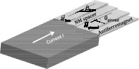
Although the physical phenomenon behind magnetoresistance is verified in simple ferromagnetic films (e.g. NiFe used in anisotropic MR (AMR) sensors), multilayered stacks (ferromagnetic/non-magnetic/ferromagnetic), such as the CoFe/Cu used in giant-MR (GMR) sensors, show enhanced resistance variations. Increasing demands on sensitivity required improved MR sensors, so in 1991 an engineered stacked structure was proposed by IBM [19], known as the spin-valve (SV) sensor. The control of the electron spins and thin-film magnetic orientation at the atomic scale has been explored since then, and present architectures are a combination of magnetoresistance with tunnel electronic transport, in a magnetic tunnel junction device (CoFeB/MgO/CoFeB, with film thickness below 2 nm—a tunnel MR (TMR) sensor). Table 1 summarizes some relevant performing indicators for these technologies. Upon proper output linearization [20], the MR device can translate the magnetic fields in their vicinity (figure 1(A)). The principles of operation and revision papers can be found throughout this paper, with a physics approach very well detailed in [21].
Table 1. Typical key properties of MR sensors: A—anisotropic, G —giant and T—tunnel.
| AMR | GMR multilayers | GMR spin-valves | TMR MTJ | |
|---|---|---|---|---|
| Thin-film structure | AMR | GMR | GMR | Spin dependent tunneling |
| Simple | Multilayers, few materials | Multilayers, several material compositions | Complex multilayers, several material compositions | |
| Buffer/NiFe/cap | Buffer/(CoFe/Cu)N/cap | Buffer/CoFe/Cu/CoFe/Ru/CoFe/MnPt/cap | Buffer/CoFeB/MgO/CoFeB/Ru/CoFe/MnPt/cap | |
 |
 |
 |
 |
|
| Thermal treatment (°C) |
Optional, 250°C–300°C | Not required | Typically 220°C–280°C | Typically 280°C –340°C |
| Linear response around zero fields | No, needs external biasing | No, needs external biasing | Yes | Yes |
| Magnetoresistance (MR) (%) |
2%–5% | 10%–100% | 6%–20% | 50% (Al2O3 amorphous barrier) |
| 300% (MgO crystalline barrier) | ||||
| Sensor linear range (mT) |
0.1–10 | 1–20 | 1–5 | 2–10 |
| Typical transfer curves | 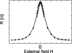 |
 |
||
aTemperature for a post-deposition/processing annealing under a magnetic field. bTypical values obtained from the sensor transfer curve (R versus B), for sensor dimensions ranging few micrometers. cThese values are registered in the literature, where an optimized linear MR sensor was reported. Notice than higher values can be achieved (e.g. 600% for MgO devices [23]), but not in a sensor configuration.
Over the past 15 years, these sensors have become essential in detecting biomolecules such as DNA and proteins, cells, vesicles and chemical analytes, when these are labeled with micro- or nanometer-sized magnetic particles [10, 14, 16]. Large and dense MR sensor array biochips were used for bio-assays [3, 22], DNA hybridization detection and to study kinetics in a solution [11]. The choice of the MR technology (AMR, GMR, TMR) is mostly dictated by the readiness level of these devices at the research group.
3. Microfluidics for integrated biochips
The integration of microfluidics with planar on-chip enclosing integrated electronics has been reported for many years. The integration of electrodes, coils, permanent magnets, photodiodes, sensors, filters, etc, over a flat surface is highly attractive for applications bridging multidisciplinary modules. As an example, the optical detection of fluorescent particles or magnetic detection of magnetic labels flowing inside a microchannel can include electronic sensor readout and fluidic handling. A thorough revision of the techniques and approaches developed in the miniaturization of bioanalysis technologies using microelectronics can be found in [24]. The technologies used for chip fabrication provide accuracy in dimensions, reproducibility of the physical mechanisms and scalability (therefore, affordability). On the other hand, microfluidics are often produced with techniques and methods not compatible with those used for semiconductor and rigid electronics industries. That is why combining microelectronics with microfluidics demonstrated to be an exciting challenge with high reward.
Since biomedical applications are closely linked with handling, manipulating and detecting fluidics or soft biological tissues, the compatibility with MR sensor technologies brings new technical challenges. In biomedical detection, sensors are expected to operate at their sensitivity limits (e.g. detecting ultra-low field from nanoparticle in flow) therefore the sensor packaging has to be redesigned to reduce the separation to the magnetic field sources. This results in direct contact between the microfabricated sensor chip and the fluids containing magnetic nanoparticles (MNPs), without further plastic encasings needed for non-biological related magnetic field detection.
Reversible or permanent bonding can be employed to integrate MR sensor chips with microfluidic modules (including, but not limited to, polymers) to avoid leakage of fluids. In the particular case of polydimethylsiloxane (PDMS), sealing of microchannels is carried out by applying pressure driven forces [25, 26], while permanent bonding is achieved through activation via oxygen or ultraviolet/ozone plasma of both PDMS and substrate surfaces before bonding [27]. Examples of Si-based biochips comprising microfluidics and MR sensors sealed in this manner can be found in [15, 28].
Reversible bonding allows the use of pico- or nanoliter automatic dispensers for multiplexed spotting and functionalization of the sensors, before placing the microfluidic module in tight contact with the chip surface. Furthermore, PDMS channel modules can be reused multiple times for different biochips, although they are more prone to potential misalignment. Additional drawbacks include (for example) the need for trapping structures over the sensing regions designed to immobilize the dispensed droplets. Permanent bonding, on the other hand, is not so well suited for multiplexed immobilization due to limited number of individual microchannels. Still, its ready-to-use nature and consistency of measurements when using different biochips, as well as reduced risk of fluid leakage during an experiment, makes this approach very attractive.
Chu et al recently published a new method to perform reversible or irreversible microfluidic bonding making sole use of an adhesion layer to seal the PDMS to a substrate, thus avoiding extra components or processing steps, or the need for plasma activation [29]. Although it is a very recent methodology, if extended to bonding between MR sensors and microfluidics on LOC platforms it may represent an alternative path to overcome some of the issues described above, making integration easier and lowering the costs.
The merging of microelectronic chips with microfluidic elements is an opportunity for the biomedical fields. The existing solutions are dedicated to solving specific problems and covering the existing technologies developed by the researchers worldwide. The following sections will describe selected applications where the use of hybrid technologies could provide a solution to biomedical challenges.
4. Combining hybrid technologies
4.1. Application 1: MR probes for biomedical purposes
4.1.1. Sharp probes for neural signal detection.
Detection of low-frequency biosignals together with the recognition and tracking of single bio-molecules have been in the spotlight of biomedical applications. Extracellular electrophysiologytechniques have been widely used to record the electric potential of biological media, such as muscular fiber or neural electric signals, and are now also an important source of information for the development of neuromorphic computational methods [30]. Distinct techniques are available to record the neuronal activity: (i) optical methods, based on light activation/inhibition [31]; (ii) intracellular electric measurements, where the plasma membrane is penetrated with sharp glass microelectrodes or by whole-cell patch clamp technique [32]; (iii) chip-based transistor techniques [29, 30]; and (iv) magnetic recording [35–37].
Microelectrode arrays are commonly used for in vitro extracellular recordings on a large area to pattern the electric activity of neuronal cells [38, 39]. The microelectrodes can be fabricated with different metal thin-films, such as Pt, Au, TiN, ITO, into substrates of Si3N4 or more commonly Si wafers, or can even be fabricated with carbon nanofibers [40]. Today, the fabrication of Si-based microelectrode arrays is an established technology [41]. One can find devices defined in small areas such as triangular probe tips with very high electrode density (figure 2(A)) [42, 43] and integrated with CMOS (figure 2(C)) [44], double-side fabrication taking full advantage of the available surface area [45], or 3D probe arrangements (figure 2(B)) [46]. More recently microelectrodes were fabricated with diamond, having lower background signal [47]. A detailed review on the existent technologies for microfabricated electrodes used in neural signal recording can be found in [30].
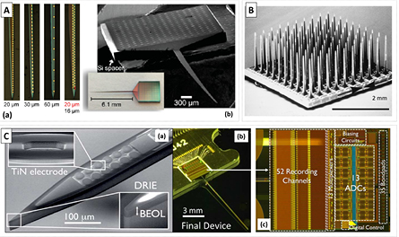
Figure 2. (A) (a) Microscope images of different Si probe electrodes designed for minimally invasive high-density neural probes and (b) SEM and microscope images of the same probe mounted on a silicon spacer for 3D stacking. Adapted with permission from [41]. Copyright 2016 American Chemical Society. (B) SEM image of the Utah Intracortical Electrode Array. © 1999 IEEE. Reprinted, with permission, from [46]. (C) (a) Image of the CMOS active neural probe; (b) SEM image of the probe with electrodes and final fully integrated and packed device. © 2014 IEEE. Reprinted, with permission, from [44].
Download figure:
Standard image High-resolution imageIn addition to electrical measurements, the bio-magnetic recordings allow reference-free and coherent measurements, since the signals of interest are not affected by the dielectric properties of the biological medium. However, the low-intensity signature of the signals requires the magnetic sensing elements to be placed as close as possible to the field sources. The first generation of devices including MR sensors displayed a 2D rigid planar geometry. In this case, the device was placed within a recording chamber and a brain slice was placed over it [35]. A step ahead was taken when the magnetic sensors were defined on top of sharp Si probes capable of being inserted in living tissue, reducing the damage to the biological medium [48]. These MR probes guarantee that the signal source and the recording elements were at a minimum distance among themselves. The active sensing area was composed of an array of MR sensors, either SVs or magnetic tunnel junctions (MTJs) [7], placed at the tip of micromachined sharp probes, displaying overall micrometer spatial resolution and high sensitivity to detect the small magnetic fields produced by ionic currents [35]. A critical point in this approach is to ensure biocompatibility between the probe and biological medium where it is immersed. The described tools targeted the development of compatible microfabrication methods for new biomedical platforms suitable for mapping of neural activity with high spatial resolution. The versatility of these tools also allow its usage outside bio-fields, namely for MR microscopy [49].
In the present section we address the main advantaged and challenges of integrating MR sensors in machined Si probes as those existing for electrical signal recording, exploring their application for the accurate detection of very low magnetic signals.
4.1.2. Integration of MR devices on Si probes.
The fabrication of probes with integrated MR sensors can be divided in two main steps: (i) sensor deposition, microfabrication and passivation, all performed on commercial Si wafers and (ii) Si probe definition and micromachining. While the former is similar for all fabricated probes, the latter is modified according to the thickness of the Si substrate (700–200 µm or 50 µm). This parameter sets the penetration depth of the probe, and together with the final tip angle is a major parameter to take into account when reducing the damage these devices may inflict in tissues.
Figure 3 shows examples of MR devices on Si probes. Each probe includes two independent recording MR elements (defined as a single sensor or an array) and an Au electrode for simultaneous electrical measurement of the synaptic signals. The probe dimensions are dependent on the sensing elements footprint and specification of the experiments. Long and wide probes (length = 11 mm; width = 1 mm) may incorporate arrays of 1000 MR elements connected in parallel of series (figure 3(A)-(a)), while smaller and narrow probes (length = 5.6 mm; width = 300 µm) are only able to incorporate individual sensing elements (figure 3(A)-(b)).
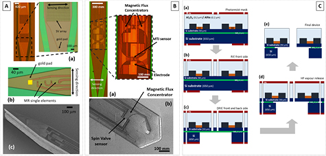
Figure 3. (A) Optical microscope image of a sharp Si probe (tip angle = 18°) with integrated MR sensing elements: (a) arrays of 1000 MR sensors connected in parallel to series recessed from the tip and (b) individual MR sensors closer to the tip. The arrows indicate the device sensing direction. (c) SEM image of a fabricated 200 µm thick Si probe incorporating individual MR elements in the tip region. (B) (a) Optical microscope image showing the integration of funnel-shaped magnetic flux concentrators (MFCs) with MTJs recessed from the tip of sharp Si probes and (b) SEM image of a fabricated Si probe with MFCs coupled to SV sensors. (C) Schematic view of the fabrication process to define the probes using SOI substrates: (a) photoresist mask definition; (b) RIE to remove the Al2O3/AlNx passivation layer; (c) DRIE performed in both wafer sides to remove silicon, and (d) device release using HF vapor to remove the 2 mm of SiO2 between the silicon layers; and (e) final device.
Download figure:
Standard image High-resolution imageFurthermore, in applications requiring a reduced penetration depth to cause minimum damage to the biological environment and where the sensing elements are placed on top of the bio-sample (e.g. in vitro experiments using rat hippocampus brain slices), a flat tip with an angle of 104° is used (figure 3(B)-(b)). However, if one needs to place the sensing elements as close as possible to the field sources (e.g. in vivo experiments), a sharp tip with an angle of 18° is selected, enabling penetration within the biological medium with reduced damage, but only incorporating individual MR elements (figure 3(A)-(c)).
4.1.2.1. MR sensors definition.
Both SV and MgO-based MTJ sensors have already been incorporated in Si sharp probes. Details on the materials and processes can be found in [48]. The sensors were patterned in rectangular shapes (typical dimensions: a few to hundreds of µm2) by optical lithography and ion milling, being defined as single elements or large arrays. Electrical contacts and leads of 300 nm AlSiCu films protected with 15 nm TiWN were defined by lift-off. The number of patterned elements affects the performance of the final device. For example, while a better spatial resolution is obtained for a single sensing element (a footprint of a few microns), the use of a large array of elements provides a signal-to-noise ratio enhancement proportional to √N, where N is the total number of elements (a footprint of hundreds of microns) [54].
To avoid the corrosion of MR sensors and contacts when in interacting with the biological medium, an optimized thick passivation of sputtered Al2O3 (200 nm)/AlNx (200 nm) bilayer, was used [48]. The electrode of sputtered Cr (5 nm)/ Au (200 nm) is patterned (20 × 20 µm2) by optical lithography and lift-off. Au being inert to the majority of the chemical reactions, having a high electrical conductivity and a higher resilience to corrosion, ensures the required biocompatibility.
Notice that MR probes can be fabricated with different sensing directions, i.e. sensitive to in-plane magnetic fields along the probe length and/or sensitive to in-plane fields along the probe width. This is an advantage since in both in vivo and in vitro experiments the generated magnetic field has an unknown direction. Within the same batch/wafer one can set the sensing direction of the MR device and change the orientation of the micromachined probe. In this case, two probes need to be used in a single experiment. The definition of MR sensors with relative 90° sensing direction within the same probe is also possible using consecutive stack depositions [7].
Further improvement of MR sensor performance atop Si probes can be achieved by coupling them to MFCs, consequently increasing its sensitivity without noise addition [50, 51]. Figure 3(B) shows the integration of MFC on MR Si probes, patterned on the sides of the sensors by photolithography and lift-off. The achieved sensitivity gain depends on the MFC geometrical dimensions (large pole/entrance ratio, length) and magnetic properties. Therefore, the probe width limits the concentrator dimension affecting the overall gain, and depending on the probe angle obliges the sensor to recess from the tip (figure 3(B)). Still, using MFCs coupled to SVs (MTJs) on micromachined Si probes we achieved a sensitivity enhancement of ~10 times improving the minimum detection level to 1.9 nT (√Hz)−1 (283 pT (√Hz)−1) at 30 Hz.
4.1.2.2. Micromachined Si probes.
The Si probe shape is defined combining two etching processes: (i) reactive ion etch (RIE), to remove oxide passivation layers (Al2O3/AlNx) and (ii) deep RIE (DRIE) to etch the entire Si thickness of the substrate, detaching probe from substrate. Two different substrates are considered, namely Si wafers with thicknesses from 200 to 700 µm (figure 3(A)) where the entire fabrication process is performed on the wafer frontside, and silicon-on-insulator (SOI) wafers, achieving a final probe thickness of about several tens of micrometers, requiring both front and backside fabrication (figure 3(C)).
The layout of the Si thick probe is defined in a 7.5 µm positive photoresist suitable for RIE, which patterns a hard mask on the unprotected passivation layer Al2O3 (200 nm)/AlNx (200 nm). DRIE of the Si probe shafts is then performed using a Bosh process, alternating etch and passivation cycles for high aspect ratios.
To deliver enhanced flexibility to the yet rigid Si-based probes, a thinner substrate can be employed. SOI substrates have been successfully used for microelectrode fabrication, down to an effective final probe thickness of 15 µm (figure 4(B)) [42]. MR probes result from an SOI wafer composed of Si (650)/ SiO2 (2)/Si (50) (thickness in µm). Figure 3(C) shows a schematic view of the SOI probe definition process, illustrating the cross section of the device in the main fabrication stages, and figure 4(C) shows an SEM image of the final fabricated and detached probe. In this case, the process described above is performed on both sides of the wafer. Two lithography steps are thus needed to define the probe shape (wafer frontside and backside), requiring controlled front-to-back alignment. On the backside, a 50 nm of Al2O3 was deposited and patterned by lithography and RIE. Finally, first a slow 50 µm DRIE is performed on the wafer frontside followed by a faster 650 µm DRIE on the backside. In order to remove the insulating middle layer of SiO2 a HF gas-phase etching is done. At the end the MR sensors are on a probe with a thickness of 50 µm.
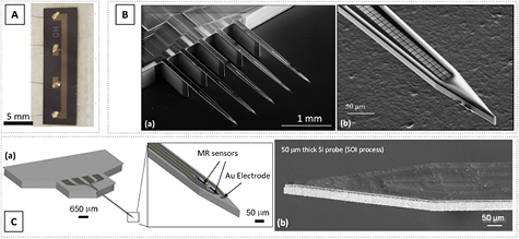
Figure 4. (A) Picture of the GMR multilayer sensors defined in a thinned Si substrate using grinding. Reproduced from [53], with permission of AIP Publishing. CC BY 3.0. (B) (a) SEM image of an array of five Si probes (total 1000 electrodes) fabricated from an SOI substrate. After the backside Si removal, each probe has a thickness of 15 µm (handling area: 510 µm thick). (b) Detailed SEM image showing the tip region with a thickness of 15 µm and a width of 50 µm. The two lines of 100 square electrodes is also visible. © 2016 IEEE. Reprinted, with permission, from [42]. (C) (a) Schematic view of an SOI-based Si probe, highlighting the tip (50 µm thick) with the integrated MR sensing elements. (b) SEM image of the final device focused on the probe tip.
Download figure:
Standard image High-resolution imageSOI SV probes showed non-degradation of magnetic properties through the fabrication process with a magnetoresistance of ~6% and sensitivity of 1.6% mT−1. However, higher noise levels compared to MR sensors on thick Si probes were observed, leading to a minimum detectable level of ~500 nT Hz−1/2 at 30 Hz, which may limit applicability.
Bending tests on Si and SOI probes were addressed by upwards/downwards mechanical displacement of the tip regarding its handling base, inducing a compressive/tensile stress in the MR elements [52], with no observed change in the noise level of the device. The influence of the magnetostriction upon bending was observed to be consistent with other works [53], but tuned correctly it improved sensitivity [52]. Perez et al used a distinct way to achieve MR sensing elements on top of thin Si substrates (figure 4(A)) [53]. The GMR multilayers were first patterned by optical lithography and lift-off on 525 µm thick Si substrates. This thickness was then mechanically reduced to 50–100 µm using grinding. The device showed resilience to 100 consecutive bending cycles, but it also showed a broadening in the output signal associated with a magnetostrictive component arising from the multilayer stack.
4.1.3. Beyond rigid Si probes.
The described Si-based probes show mechanical robustness, and starting from common Si wafers are suitable to grow high quality MR stacks and are highly compatible and easily scalable with standard microfabrication tools and processes. Profiting from their miniaturized size, additional features, such as localized drug delivery [46, 55–57] or precise sample analysis [58, 59], can be accomplished by integrating microfluidic channels (figure 5(A)). This matching is possible by combining Si compatible surface and bulk micromachining techniques as described in the following two examples [55]. Lin et al developed a microchannel on top of a 50 µm thick Si microneedle enclosing resistive heaters as pumps and an inlet/outlet at each end of the channel [56]. The microchannel atop the probe is defined by a sacrificial layer of phosphorus-doped glass (PSG) which acts as the mold, being covered by SiN. The PSG is then etched away with concentrated HF defining a microchannel of 50 µm width and 9 µm height along the entire probe length (1–6 mm). Moreover, Lee et al demonstrated the integration of buried channels in the Si probe [57]. Starting from an SOI wafer, cylindrical channels with 20 µm inner diameter are enclosed within SiO2 using optical lithography, DRIE and isotropic XeF2 etching, and sealed with polysilicon avoiding the need of alignment (figure 5(B)). Each silicon probe (11 mm long, 84 µm wide, 70 µm thick) has two incorporated independent channels, allowing simultaneous fluidic injection and sampling. The authors state that ~150 probes were fabricated in each run on a 4 in. wafer, although challenges such as accumulated intrinsic stress and mechanical fragility of the structures were present. To match the external fluidic capillaries with probe internal microchannels a customized holder and capillary guides were efficiently used.
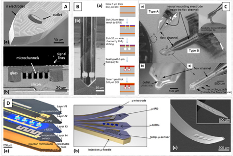
Figure 5. (A) SEM images of Si microneedles enclosing microchannels showing (a) the tip of the shank with microelectrodes and outlet, and (b) a cross section with enclosed microchannels. Adapted from [55] with permission of The Royal Society of Chemistry. (B) (a) Process steps to achieve cylindrical channels buried in oxide starting from an SOI wafer and (b) an SEM view of the machine channels and probe. Adapted with permission from [58]. Copyright 2013 American Chemical Society. (C) Examples of a flexible parylene probe integrated with a flexible parylene microchannel as described by Takeuchi et al. Reproduced from [59] with permission of The Royal Society of Chemistry. (D) (a) The multifunctional and implantable optoelectronic device highlighting the various components designed by Kim et al [64], (b) illustration of the printed multifunctional system and (c) SEM of the injectable array with inset showing the rigid device before passivation. From [64]. Reprinted with permission from AAAS.
Download figure:
Standard image High-resolution imageEven more functionalities can be explored using flexible substrates, which offer the advantage of reduced mechanical mismatch between the sensing device and tissues [30], thus less invasive than conventional rigid Si-based probes. In fact, several flexible substrates have already been used with success for the fabrication of neural probes with microelectrodes, e.g. parylene [59, 60], polyimide [61, 62] and PDMS [63]. The capacity to fabricate electrode arrays in extremely dense arrangements down to 50 nm pitch, by combining these polymers with electron beam lithography, has also pushed their performance further [60].
Kim et al put all these fabrication methods together and demonstrated a multifunctional operation probe system which includes a myriad of features, namely stimulation (optical), sensing (microelectrodes, temperature sensors, optical sensors) and actuation (injection needle) within a bendable approach (figure 5(D)) [64]. Moreover, fluidic channels are also integrable in flexible probes for fully flexible devices [59, 63]. Takeuchi et al introduced a flexible microfluidic probe made of parylene enclosing Au electrodes and a channel width of 50–200 µm (figure 5(C)) [59]. The fabrication of the polymer device is performed using a handling Si wafer with conventional micropatterning tools and processes. The fact that the probe and microchannel are fabricated on the same polymer readily places the electrode inside the fluidic channel, but also facilitates sealing/bonding which can be improved by thermal bonding [65].
Combining all these advantages, one can move towards the inclusion of MR sensors within flexible probes offering additional characterization capabilities. In a recent paper, Gaspar et al describe the fabrication details to achieve high performance TMR devices in polyimide probes [66] for neural applications. The overall challenges and routes necessary to develop such MR-flexible technology are discussed in detail in section 4.2.
4.2. Application 2: magnetic sensor integration in shapeable substrates
4.2.1. MR sensors on flexible substrates.
Great efforts have been made in recent years toward delivering high-performance flexible MR devices, aiming at similar progress as in wearable electronics [67], flexible photonics [68] and energy storage devices [69]. Compared to those, the fabrication of spintronic sensors shows unique technical challenges [70, 71] due to the demanding nanomorphology constrictions, such as a continuous layer less than a few nanometers thick and a highly controlled roughnesses of ⩽1 nm.
The first demonstration of MR materials on polymer substrates was performed at IBM [72] using exchange biased structures deposited on, e.g. kapton. At that time, the focus was on MR magnetic recording read heads, which could be made flexible and extremely lightweight if thin and smooth flexible substrates were used.
Currently, significant progress has been made in flexible spintronics targeting multifunctional sensing devices, using single ferromagnetic layers with AMR (figure 6(A)) [73], GMR multilayers (e.g. Co/Cu) [71, 74, 75], the Hall effect (figure 6(B)) [76] and giant magnetoimpedance [53, 71, 75, 77, 78]. These sensors have been demonstrated for a wide range of applications, such as wearable devices, position sensing, magnetic switches, and stretchable devices, among others [75]. One resorts to distinct techniques to assemble the devices either by combining standard microfabrication methods (sputtering, optical lithography, liftoff, etc) with the rigid handling of the flexible media [66, 69] or printing (e.g. inkjet) directly onto the polymer [71, 75]. A detailed review of the technology, fabrication processes and applications can be found elsewhere [79].
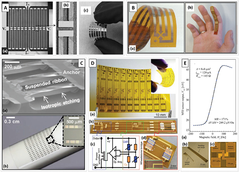
Figure 6. Examples of flexible magnetic sensors. (A) (a) AMR sensors patterned in a Wheatstone bridge configuration on a flexible substrate, (b) zoom over the barber poles on the NiFe layer, and (c) the AMR sensor on a flexible PET foil. [73] John Wiley & Sons. © 2016 WILEY-VCH Verlag GmbH & Co. KGaA, Weinheim. (B) (a) Flexible Hall sensor which can be (b) conformed to a finger. [76] Copyright Wiley-VCH Verlag GmbH & Co. KGaA. Reproduced with permission. CC BY-NC 4.0. (C) (a) Si undercut etching under the fabricated and annealed MgO structures for transferring to the (b) flexible substrate. [82] John Wiley & Sons. © 2016 WILEY-VCH Verlag GmbH & Co. KGaA, Weinheim. (D) (a) Array of flexible GMR sensors and electronics fabricated on 50 µm polyimide foil and (b)–(d) details over the complete system. [85] Copyright Wiley-VCH Verlag GmbH & Co. KGaA. Reproduced with permission. CC BY-NC 4.0. (E) Representative TMR output of a 8 × 8 µm2 MgO-MTJ pillar with stack (Ta (5)/CuN (25)) × 6/Ta (5)/Ru (5)/MnIr (20)/Co70Fe30 (2)/Ru (0.85)/CoFeB (2.6)/MgO (1.0)/CoFeB (2)/ Ta (0.21)/NiFe (4)/Ru (0.2)/MnIr (6)/Ru (2)/Ta (5)/Ru (10) (thickness in nm) fabricated and annealed on polyimide substrate; the inset shows an example of released structures and single sensor design. Reproduced with permission from [66]. © Copyright 2017 IEEE.
Download figure:
Standard image High-resolution imageAnother class of MR sensors such as SVs and MTJs require a well-defined reference layer, allowing linearization of the sensor output [7, 20]. For these complex stacks, where functional layers include exchange biased pinned layers and synthetic antiferromagnets for improved performance and well defined magnetic reference, accurate control of the layers' thickness, defects and roughness is most critical. One major issue is to reduce the impact of the substrate roughness on sensor performance, where buffer layers of photoresist [73] or sputtered thick bottom electrode films [66] can be used.
SV with top-pinned reference were demonstrated in PDMS substrates for stretchable sensors [80]. Li et al showed top performing SV sensors compose of Ta buffer/MnIr (10)/CoFe (4)/Cu (3)/CoFe (1)/NiFe (6)/CoFe (1)/Cu (3)/CoFe (4)/MnIr (10)/Ta cap (thickness in nm), sputter deposited onto pre-strained PDMS substrates with MR = 9.9% and a field sensitivity up to 6.9% mT−1. As for MTJs, the first examples on flexible substrates were put forward recently [66, 70, 81, 82]. Since MTJs rely on the tunneling magnetoresistance (TMR) effect, sub-nanometer deposition requirements regarding both thickness and surface roughness are essential. Therefore, the task of integrating MTJs on flexible substrates is a major challenge and to date only a few examples exist [70, 81, 82], fewer with stack integration of an exchange-biased reference layer [66]. MTJs based on Co/Al2O3/Co [81] and Co/Al2O3/NiFe [70] deposited on 300 µm polyimide films showed TMR of 12.5% and 8% at room temperature, respectively. Al2O3 barriers compared to MgO, although yielding lower TMR values, are advantageous for these strategies due to their amorphous nature, thus avoiding the need for high temperature annealing [83].
For MgO-based stacks, a critical high-temperature annealing step is mandatory to achieve coherent tunneling and large TMR values at room temperature (>100%) [84]. Loong et al showed flexible MgO barrier MTJs fabricated using transfer printing (figure 6(C)) [82]. They start by depositing the stack buffer/CoFeB (6)/MgO (2)/CoFeB (4)/cap (thickness in nm) on rigid Si wafers with a thick SiO2 layer, which acts as a support upon release from the substrate. The micropatterning of the MTJ structures and annealing (>300°C) are performed while the stack is still on the rigid Si wafer. The Si substrate is then removed by combining isotropic wet etching and RIE, leading to suspended structures. A PDMS stamp is used to fully remove and handle the released MTJ structures, which are then transferred to, e.g. PET substrates [82]. Here, polyimide substrates make a difference as they are more resilient to high temperatures and thus compatible with MgO-MTJ annealing steps (>250 °C). Gaspar et al reported MgO devices with synthetic-antiferromagnetic (SAF) pinned-reference and weakly pinned sensing layers fully fabricated and annealed on polyimide substrates and displaying TMR above 150%, exceeding most reported values (figure 6(E)) [66]. A Si wafer is used to handle the spin-coated polyimide for compatibility with clean room microfabrication tools. The fully fabricated structures are released only at the end of the process without any loss in their performance. Final devices yielded field detection values fully in line with most competitive and state-of-the-art rigid TMR sensors [7].
These results open the door for viable devices with a robust, uniform and reproducible fabrication process which facilitates integration with other technologies such as microfluidics, conditioning electronics and optics. A step towards fully flexible integrated MR devices was demonstrated by Münzenrieder et al [85]. Figure 6(D) shows such solution enclosing GMR sensor and acquisition electronics, both defined in a 50 µm polyimide foil. The sensor consists of sputter deposited GMR Co/Cu multilayers in Wheatstone bridge patterned by optical lithography and lift-off (meanders of width = 10 µm, length = 38 mm). Electronic components were also defined by standard fabrication (UV lithography, wet etching, lift-off). Passivation was achieved using a customized polymer in detriment of highly conformal atomic layer deposited Al2O3 which, according to the authors, yielded pinholes in millimeter size areas [85]. Benefits include the high gain of the readout electronics and the high signal-to-noise ratio. Most importantly, this approach goes beyond more routine methods, where the flexible–rigid connections are achieved using cables or mechanically flexible interconnects [86].
4.2.2. Fully flexible solutions for magnetic detection and actuation of particles.
One direct use of flexible MR sensors is in combination with polymer microfluidic platforms, to provide entirely flexible and integrated solutions. Lin et al demonstrated the first flexible microfluidic device with integrated GMR sensors targeting flow detection of magnetic particles on droplets (figure 7(A)) [87]. The sensors relying on NiFe/Cu GMR multilayers were fabricated in a 100 µm PET foil and passivated with crosslinked SU-8. The authors highlighted the fact that brittle oxides as SiO2 or Al2O3, common for passivation layers in rigid MR biosensors (examples in sections 4.1 and 4.4), were not used. Here, the encapsulation in a polymer not only ensures that flexibility is maintained but, in this case, also facilitates bonding. The PDMS microfluidic channel with 100 µm width was casted from a SU-8 mold, and then permanently bonded to the SU-8 passivated GMR sensor, using N2 plasma treatment and heat. Proof-of-concept was achieved using emulsion droplets enclosing superparamagnetic ferrofluid 10 nm nanoparticles with distinct concentrations, detecting peaks as single droplets pass over the sensor (figure 7(A)).
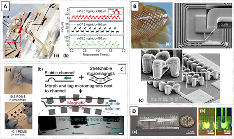
Figure 7. Examples of flexible structures for magnetic detection and actuation (A)–(C). (A) (a) Image of an entirely flexible GMR-microfluidic device filled with liquid and droplets submitted to a bending radius. The inset shows the emulsion droplets inside the microfluidic channel and (b) the output signal of the device detecting the flow of magnetic droplets, with different concentrations of encapsulated MNPs. Reproduced from [87]. CC BY 3.0. (B) (a) Example of microcoils defined on polyimide substrates with (c) 2D square-shaped microcoils and (b) 3D microsolenoids. Reprinted from [88]. Copyright 2006, with permission from Elsevier. (C) Ferromagnetic microstructures in PDMS with (a) different thicknesses and elasticities, and (b) an illustration of the concept of this stretchable micromagnet array to control the path of magnetic particles with selected frames of real manipulated particles against the direction of fluidic flow. [90] John Wiley & Sons. © 2014 WILEY-VCH Verlag GmbH & Co. KGaA, Weinheim. (D) Example of a non-conventional use of polymer flexible microfluidics for electrical connections to an integrated circuit showing (a) the final device and (b) a detail of the empty microfluidic channel over the contact pad and corresponding channel upon the filling with conductive liquid. Reprinted with permission from Macmillan Publishers Ltd: Scientific Reports [92], copyright 2013.
Download figure:
Standard image High-resolution imageWoytasik et al validated the fabrication process for both 2D and 3D microcoils on flexible polyimide and PEEK substrates [88] (figure 7(B)). The steps included standard and 3D optical lithography of 18 µm thick photoresist for the definition of the patterns, which are then filled with Cu grown by electrodeposition. Technical limitations are mostly focused on the aspect ratio and contrast of the photoresist, and resolution in the lithography alignment, which limit the minimum size of the patterned microcoils [88]. This approach highlighted the compatibility of the polyimide with electrodeposition. Although they targeted the demonstration of three-axis magnetic sensors, these structures may be extended to particle trapping and actuation similar to Fulcrand et al [89]. In the latter case, the authors demonstrated a stretchable micromagnet array for actuation in a microfluidic system embedding planar microelectromagnets showing efficient trapping of microbeads without the aid of any external field source. The device was fabricated on PET, which was handled on a Si wafer using laminated adhesive and the coils are defined on top by SU-8 lithography and Cu electroplating [89]. Ferromagnetic elements fabricated in flexible PDMS films have also been used to manipulate magnetic particles within microchannels (figure 7(C)), where different pathways can be tuned according to the changing shape of the PDMS–magnetic substrate [90].
Beyond medical devices, the more unconventional use of polymer-based microfluidics in electronics [91], electrical connections for integrated circuits (figure 7(D)) [92], memories, multiplexers and logic devices [93], and tactile sensors [94] may prompt even further the use of flexible platforms for multifunctional applications also including magnetic devices, as highlighted in a recent review [94].
4.2.3. Integration of 3D shaped MR sensors with microfluidics.
Beyond fully flexible devices, other strategies use shapeable thin-films via strain engineering [95] to put together MR sensors and microfluidic platforms. The 3D shaping of planar MR sensors using strain engineering profits from accumulated stress in deposited films over sacrificial layers, making the fabricated structures roll into tubular architectures upon release (figure 8(A)) [95, 96]. A detailed overview of the use of lab-in-tube strategies for total analysis systems, besides magnetic-based devices, can be found elsewhere [97].
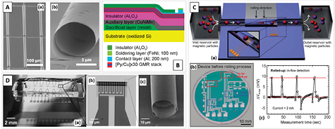
Figure 8. (A) SEM image of micro-scale tubular architectures. Reprinted with permission from [100]. Copyright 2016 American Chemical Society. (B) Schematics of the layered stack for the roll-up process with GMR sensors described by Monch et al. Reprinted with permission from [98]. Copyright 2011 American Chemical Society. (C) (a) Drawing of the full concept for detection of flowing magnetic particles using the rolled-up sensing tubes by Monch et al; (b) image of the planar microfabricated device on a wafer before assembling the tubes with highlights on the distinct parts composing the bridge sensors; and (c) device output for magnetic particles flowing within the tube, where each peak corresponds to a particle passing through a sensor. Adapted with permission from [98]. Copyright 2011 American Chemical Society. (D) General view of a final bio-device with microelectrodes (not magnetic sensors) to highlight the tubular sensing structures placed within a PDMS microchannel which provides the inlet and outlets for the fluids. Adapted with permission from [102]. Copyright 2016 American Chemical Society.
Download figure:
Standard image High-resolution imageFigure 8(B) shows the schematics with the layer stacking employed in the roll-up process [98]. Starting on Si wafers, a photoresist sacrificial layer is deposited on a pre-defined area, followed by 100 nm CuNiMn for the rolling up. An Al2O3 passivation layer is deposited prior to the GMR multilayers, which is then microfabricated using optical lithography and lift-off. The roll-up procedure is performed using acetone and their geometry determined by the area defined for release (setting the length) and by the strain imposed to the multilayers via materials used and deposition conditions (setting the diameter) [99]. Monch et al used strain engineering to roll-up a GMR multilayer magnetic sensor into tube diameters of 60 µm with a total length of 15 mm [98]. The final sensors form a bridge configuration, with two rolled-up meanders and two planar sensors with a reported (differential) sensitivity of ~2.3% mT−1 (figure 8(C)) [98]. The device performance is demonstrated for dynamic detection of flowing ferromagnetic CrO2 MNPs encapsulated into a hydrogel shell with final diameter of ~40 µm. An example of the output is shown in figure 8(C) where each peak corresponds to a single particle.
These tubular magnetic structures are also being used for particle manipulation. Ueltzhöffer et al used these structures (inner diameter of 10 µm) enclosing exchanged-bias continuous thin-films with customized stripe domain structures via ion bombardment [100]. Using external weak magnetic field pulses to control the movement of the domain walls, this pattern allowed one to move superparamagnetic microbeads in an aqueous solution in a controlled path inside and along the outside of the microtube [96]. In a recent review, Streubel et al discuss the potential and possibilities arising from exploring the particularities of magnetism in curved shapes [101].
Still, and according to the device depicted by Medina-Sánchez et al [102], these tubes are not yet standalone and inlets and outlets are provided by, e.g. routine PDMS microchannels (figure 8(D)), as described in section 3. In contrast, a clear advantage arises if the size of the beads and the diameter of the tube are tuned accordingly, for only one magnetic particle will pass through, enabling the distinguishable counting of single particles, as shown by Monch et al [98].
4.3. Application 3: magnetic sensor integration with paper microfluidics
4.3.1. Overview of paper microfluidics for bio-applications.
Another alternative flexible technology relies on paper microfluidics [94, 103, 104, 106], and presents unprecedented easy-to-use solutions in point-of-care (POC) testing (figures 9(A)–(C)) [103, 107, 108]. Paper substrates are low-cost and readily integrated with large-scale and cost-effective fabrication methods such as printing [110–112]. Systems based on this technology also offer the prospect of reduced material consumption and biodegradation, suitable for greener bio-solutions [112]. All this combined increases the potential of paper microfluidics not only as a standalone method, but also as a vehicle to integrate distinct technologies.
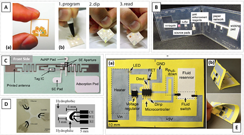
Figure 9. Examples of paper microfluidic applications. (A): (a) Concept of microfluidic paper-based analytical devices (µPAD). Reprinted with permission from [104]. Copyright 2009 American Chemical Society. (b) Strategy used for a programmable µPADs for urinalysis. Adapted from [105] with permission of The Royal Society of Chemistry. (B) A 2D paper network card for an amplified immunoassay. Adapted with permission from [109]. Copyright 2012 American Chemical Society. (C) Self-powered RFID biosensor prototype integrating paper-based microfluidics and a self-assembled RF antenna. © 2016 IEEE. Reprinted, with permission, from [117]. (D) Image and schematic design of the electrode paper-based microfluidic device demonstrated by Dungchai et al. Adapted with permission from [114]. Copyright 2009 American Chemical Society. (E) Paper-based integrated system incorporating fluidics and electronic components, with wiring connections fabricated in paper and (b) image of the folded paper circuit. [118] John Wiley & Sons. © 2016 WILEY-VCH Verlag GmbH & Co. KGaA, Weinheim.
Download figure:
Standard image High-resolution imageStill, only few paper-based microfluidics offer fully integrated solutions for quantitative biomolecular detection, mostly for (electro)chemical sensing [114]. The fabrication of these structures is compatible with paper, since channels can be patterned by lithography, inkjet printing or wax printing, and combined with printing of conductive inks to define electrodes [113]. Dungchai et al used SU-8 (hydrophobic) lithography to define the microfluidic channels and screen-printing to define the electrodes (figure 9(D)) [114]. Outside bio-applications, Yuan et al showed inkjet printed RF antenna patterned on a plastic substrate integrated with laser cut microchannels on paper (figure 9(C)), proving the concept using an RFID tag. This approach stands out, as it brings together two flexible technologies, paper–polymer, with clear added benefits [117]. Finally, the use of paper-based technologies was successfully demonstrated as a means to integrate electronics and microfluidics (figure 9(D)) [118]. This strategy allows bridging distinct technologies, opening new routes to increase the number of added functionalities, to include batteries, electrochemical actuators or sensing devices, as outlined by the author [118].
4.3.2. Lateral flow devices.
A particular case of paper-based microfluidics is lateral-flow testing (LFT), which became popular as rapid diagnostic tools [107, 108]. In 1984 the first commercial LFT for home pregnancy testing was launched [115], representing a major technological breakthrough in providing a simple, fast, and reliable home test tool. Ever since, this technology has been employed in rapid testing for clinical, veterinary, food industry and environmental applications, among others. Moreover, a wide range of analytes can be considered (peptides, proteins, pathogens, bacteria, etc), strengthening the versatility of LFTs. A detailed review of the practical uses of LFT can be found elsewhere [103, 107, 108, 116]. Nonetheless, most LFT devices only offer a qualitative result, i.e. presence or absence of a target analyte, significantly limiting their applicability. Design strategies and mechanisms are still required to devise quantifiable tests, hence the inclusion of external detection and/or actuation systems, which are assembled discretely or integrated with paper technology, are still necessary.
For LFT, a liquid sample is loaded and handled along a single axis on a pre-fabricated strip, without the need for pumping systems. First, the analyte of interest is labelled and the detection takes place by concentrating and purifying it in a specific region—the test line (figure 10(A)). An LFT strip usually encloses several porous membranes, biorecognition molecules (e.g antibodies) and a signal generation system/labeling mechanism [119]. The type of labels used are contingent on the detection method employed; examples are Au nanoparticles, color dye beads and MNPs [120, 121]. In nanoparticle-based LFT, the labels are typically sub-micron sized as they need to flow through the pore structure of the strip. The use of small particles, although moving faster along the LFT strip, can lead to low intensity signals, putting pressure on highly sensitive sensing tools. Still, care needs to be taken with particle property degradation, autofluorescence or artifacts from a wet LFT strip. Most common LFT systems available, with quantifiable output, are based in optical readers for reflectance or fluorescence emission (figures 10(B) and (C)) [120–124], in some cases using smartphones as an interface.
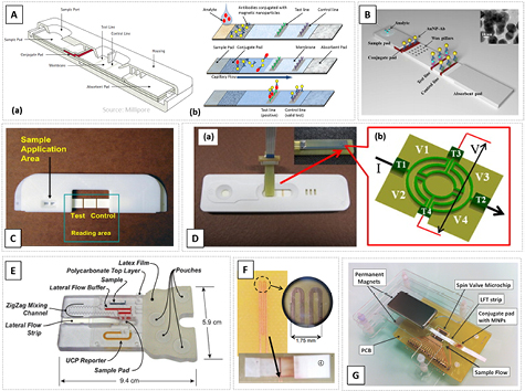
Figure 10. Examples of LTF devices. (A) (a) Schematic view of a commercial LFT [119] including a number of components and materials and (b) schematic representation of the operation of an LFT. © 2014 IEEE. Reprinted, with permission, from [134]. (B) Schematic of an LFT strip optimized for detection of Au nanoparticles using wax pillars. The inset shows a TEM image of the particles used. Reproduced from [122] with permission of The Royal Society of Chemistry. (C) LFT strip in a cartridge for MICT equipment. Reprinted from [126], Copyright 2009, with permission from Elsevier. (D) Experimental setup to detect MNPs in real time at the test line using an AMR/PHR sensor. Reprinted from [129], Copyright 2011, with permission from Elsevier. (E) Image of the assembled immunoassay cassette developed by Lui et al, a lateral flow strip for optical/color detection. Reproduced from [125] with permission of The Royal Society of Chemistry. (F) Image of the magnetic sensing circuit used by Lago-Cachon et al, and an image of the nanoparticles binding to the capture line over the sensor. Reprinted from [127], Copyright 2017, with permission from Elsevier. (G) An LFT prototype with magnetic detection comprising a microchip with two MR sensors, a lateral flow test strip, a printed circuit board (PCB) and two permanent magnets for particle magnetization © 2014 IEEE. Reprinted, with permission, from [134].
Download figure:
Standard image High-resolution image4.3.3. Magnetic sensors for LFT.
In alternative to optical detection, magnetic sensing can be employed requiring the use of superparamagnetic particles as labels. These are very stable in comparison to organic fluorescent biomolecules, and can be tuned with different sizes and magnetic content.
Previous research efforts have achieved exceptional sensitivities by incorporating a number of magnetic sensors to LFT strips to measure the MNPs [127–131]. The combination of immunomagnetic LFT and magnetic sensors potentiates the design of LFT tests with high sensitivity and spatial resolution for MNPs. Furthermore, in contrast to most optical approaches, there is no signal interference between strip materials and biological sample constituents as these are insensitive to magnetic fields. Additionally, these sensors allow automatic detection and quantification using simple algorithms. Still, most of the available systems for magnetic detection enclose discrete sensing elements (e.g. lines, coils) placed below or around the LFT test line (figures 10(C), (D) and (F)) [127–129], or need bulky systems to scan the sensor over the LFT strip [130–133]. Lago-Cachón et al showed the detection of MNPs by measuring the impedance of the sensor change (figure 10(F)) [123]. This method detects eddy currents induced on the surface of a Cu meander-line structure produced by vibrating MNPs while not requiring their magnetization.
Orlov et al introduced a new measurement system based on inductive coils [128], able to scan an LFT strip and quantify the amount of MNPs along the entire strip in 25 min with high sensitivities. Multiplexed biosensing for three analytes was demonstrated with this technique, by incorporating three separate LFTs within the same device [128]. MR sensors have also been used for LFT quantification. The first work [130] employed GMR sensors (560 µm2 active area) for the quantitative detection in immunochromatographic assays with high sensitivity. The LFT strip was scanned on the GMR sensor surface, with a constant velocity controlled by a syringe pump. Further studies [131–133] applied similar methods with GMR sensors or arrays to investigate MNP quantification, improving the limits of detection. Most of these examples require scanning over the surface of the LFT strip. While this strategy shows great improvement in sensitivity, drawbacks such as the need for a stabilized or dried test before measurement, careful sensor–LFT alignment, and positioning at a close constant proximity, arise. Another study showed an improvement of sensitivity by applying two TMR sensors in a differential configuration to scan the LFT strip in a contactless mode at a 2.5 mm height. The scan was faster than existing commercial systems [135].
Moreover, even though the system can detect particles deeper in the LFT strip, the signal obtained is dependent on the relative position of the MNPs to the sensor active area. This can lead to irreproducible results if the MNPs are not uniformly distributed in the thickness of the LFT. Finally, another shortcoming of these works is the active footprint of the sensing elements. The GMR sensors are micron-sized while the LFT strip and test line are millimeter-sized, hence the detected signal is a small fraction of the overall signal produced by the MNPs. This can be easily overcome by increasing the sensitive area, such as using a larger number of GMR sensors.
The closest solutions to an integrated paper/MR platform are introduced in [129, 134]. The first demonstrated real-time quantification of MNPs on an LFT was reported in [129] (figure 10(D)). The biosensing device used a hybrid AMR/Hall sensor of 600 µm to analyze the kinetics of mass migration and chemical reactions. This work showed unprecedented speed and real-time quantification within 1 min. A distinct approach, also for real-time detection, integrated several components in a readout platform aiming at a stand-alone, low-power and compact device [134] (figure 10(G)). In this case, SV sensors were processed on a rigid Si substrate and encapsulated on a PCB, and the LFT strip positioned in close contact with the MR sensors. Two external permanent magnets ensure a high and homogenous magnetic field for the detection of MNPs, not affecting the in-plane sensitive direction of the sensors. Superparamagnetic 10 nm MNPs were selected to minimize particle clustering which might affect their diffusion. The proposed system and detection method were used for quantification of biomolecules in LFT by monitoring the amount of MNPs flowing before and after the test line. Furthermore, the authors report that this system is inexpensive, offering a high spatial resolution tool for understanding intricate diffusion and nanoparticle flow in microporous membranes.
Finally, LFT readers based on MR sensors and magnetic labels is a promising alternative for reading beyond the visual detecting limits, achieving very good sensitivity and limits of detection with short waiting times. The inclusion of MR sensors in substrates other than rigid Si can improve the compatibility, add flexibility and may decrease the sensor's distance from the source of signal, achieving high-quality detection with increasing sensitivity.
4.4. Application 4: integrated systems for particle manipulation and detection on-chip
4.4.1. MR biochips.
Over the past 18 years, several MR-based biochips have been demonstrated as proof-of-concept systems for biological probe–target recognition detection. Apart from lateral bioassay configurations (section 4.3), where labeled target analytes drive through a paper-based porous structure, two major architectures standout. (i) Static mode devices, where probes (complementary DNA, aptamers, antibodies, etc) are immobilized on a substrate over different MR sensors, and magnetically labeled analytes interact with immobilized probes for conjugation [10–14, 16] through a microfluidic system. The analyte can be magnetically labeled, either before or after its biomolecular recognition by the probe. These labels are MNPs with a diameter from ~10 nm to ~1 µm, depending on the application and sensing geometry. Due to their dimensions, the MNPs are typically superparamagnetic with a remnant magnetic moment equal to zero preventing their agglomeration. Finally, once near the sensor area, these particles are magnetized with a magnetic field (external or generated with on-chip lines) and their fringe field is sensed by the MR sensor. (ii) Dynamic cytometer-based devices, where labeled analytes flow in a microchannel over MR sensors, targeting the detection of single analyte events without capture on the surface [28, 136, 137].
Representative solutions devised from the research and optimization on MR biochips was at the origin of three start-up companies, MagArray from Stanford University in 2005 [141], Zepto Life Technology from the University of Minnesota in 2014 [142], and Magnomics from research institutes INESC-MN/INESC-ID in 2014 [143]. The advances led them to the pre-clinical validation stage.
In addition, for static mode devices the MR sensor output voltage depends on the number of MNPs over its surface, allowing a quantitative analytical detection mode, rather than only a 'yes/no' response. This quantitative mode is defined by the dynamic range, i.e. the range separating the lower and higher limits of detection of the sensor. Because the MR sensor response is proportional to the MNP content, and consequently to the average fringe field over the sensor area, larger sensing areas will translate to smaller sensor resistance change resulting from a single magnetic particle. However, such large sensing areas enable the detection of a higher number of particles, increasing the dynamic range. Therefore, by choosing the MR sensor dimensions adequately, both the dynamic range and limit of detection of the sensors can be defined. Smaller sensors are more suited for 'yes/no' applications, while larger sensors are used in quantitative assays. MR biochips typically include less than 100 sensors. Still, in applications aiming at increased multiplexing, a larger amount of sensors may be needed. In this case, matrix-based biochips were proposed to include ~1000 sensing sites in the same chip [138, 139].
LOC systems for MNP manipulation and separation can be custom designed, aiding to concentrate or purify a desired analyte from a given sample, thus improving the detection efficiency and signal output [140]. In all scenarios, however, complementary systems integrating chambers for sample preparation, labeling, or signal amplification may be required. At this stage, the sensing and manipulation capabilities of magnetic devices are proven, but its prospective societal impact will be revealed by moving forward to the analysis of molecules, pathogens, circulating cells or extracellular vesicles, from real samples, such as blood, urine or saliva, which require additional preparation steps prior to detection. Dias et al demonstrated the pre-analytical steps required to detect relevant circulating cell-free DNA fragments from human plasma [25]. Previously, synthetic DNA fragments were frequently used in proof-of-concept using MR sensors which often neglected the real implications inherent to the analysis of bioanalytes from real samples.
4.4.2. Open-well based format configurations.
The first generation MR sensors demonstrated in bio-applications were identical to the conventional enzyme-linked immunosorbent assays (ELISA). Open-well based structures were integrated with the sensing regions of a biochip. These barriers enclosed the necessary reagents and analytes for reaction and detection, or were simply dispensed and washed sequentially over the biochip surface [12, 14, 16, 22, 144–148]. This sort of combination is extremely useful in approaches that do not require permanent integration [149], or for demonstration of new detection methodologies [150].
INESC-MN pioneered the development of MR biochips [10]. Typical sensor elements consist of two SV (2.5 × 40 µm2) connected in series, inside a U-shaped current line that is used to focus magnetically labelled target analytes over the immobilized probes (figure 11(A)). The MR structure is Si/ AlOx/Ta (1.5)/NiFe (3.6)/CoFe (2.5)/Cu (2.1)/CoFe (3.3)/MnIr (11)/Ta (10) (thickness in nm). Contact leads were defined by lithography, deposited by magnetron sputtering (AlSiCu (3 0 0)/TiW(N) (15) (nm)), with the process finished by a lift-off step. A thin Au pad (Ti (5)/Au (40) (nm), 43 × 13 µm2) was defined by sputtering and lift-off over the Si3N4 passivation and sensor structure to allow probe immobilization to the Au pad. Encapsulated sensors had a typical MR signal of 7.5%. The initial architecture had a U-shaped PDMS microfluidic channel (100 µm wide, 40 µm height) clamped over previously functionalized biochip surface (immobilized probes), where one structure was used as reference (without Au pad). Alignment of the microfluidic structure over the processed chip was done through the clamping device and reversible bonding, therefore allowing a reusable scheme for the MR chip. The main challenge in these types of platforms is the extraction of low signal-to-noise ratio signals, within a complex environment involving electrical, magnetic and biological phenomena. The portable platform controls and reads out the signals from the biochip assays [13], being able to address up to 256 biosensors and transmit the processed signals to a digital analyzer where, through a graphical user-interface, the experiment is controlled.
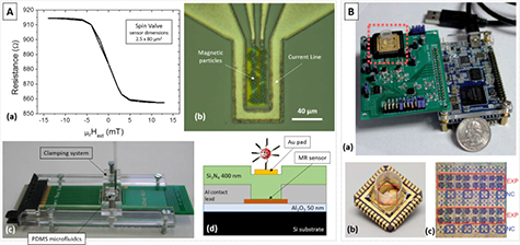
Figure 11. (A) Example of a static detection biochip from INESC-MN. (a) Transfer curve of an SV sensor. (b) Focusing method for magnetic particles using current lines. (c) Clamping device to aid bonding of the PDMS microfluidic channels and (d) cross section of the chip layout. (B) CMOS handheld diagnostic device from Pai et al [150]. (a) Device consisting of the plug-in cartridge, circuit board, and USB interface, (b) example of the disposable chip with a polypropylene well and (c) chip layout. [150] Reproduced by permission of The Royal Society of Chemistry. CC BY-NC 3.0.
Download figure:
Standard image High-resolution imageA distinct architecture of a magnetic handheld CMOS sensing platform is demonstrated by Pai et al, for antigen and nucleic acid detection using a magnetic freezing technique [150]. The device consists of a portable plug-in cartridge, circuit board and USB data interface for communication and power, which then connects to a disposable magnetic CMOS cartridges. The chips inside the cartridges have 48 sensor sites and 16 reference sensors. A well of polypropylene is used for the reaction between immobilized probes and target analytes (figure 11(B)). By employing the magnetic freezing technique the authors avoided the need for a baseline measurement before the experimental assay. Detection limits down to 100 pM for synthetic DNA and 1 pM for proteins were reported. The signal-to-noise ratio was improved when compared to a similar biosensor [149] and was able to perform output signal measurements after concluding the biological assays, which is an advantage for simultaneous incubation of various analytes on different cartridges and further sequential signal detection.
The inclusion of microfluidics and/or magnetic actuators into this handheld device is promising in allowing in situ separation, purification or labeling of target analytes for realistic POC diagnostics, avoiding the need of prior bulky benchtop sample preparation methodologies. Still, the open-well cartridge requires large sample volumes (100 to 400 µl). This is not cost-effective for most POC diagnostics due to the high cost of most reagents and the limited availability of real analytical samples. Nonetheless, these devices represent a great advance in biomedicine-related fields, opening new pathways to be customized and used in POC diagnostics.
4.4.3. Microfluidic multi-channel arrays integrated with MR sensors.
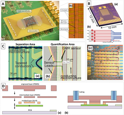
Multi-microchannel arrays integrated with MR sensors on biochip structures have been used on dynamic cytometer devices [28, 136] and (in-)flow detection [87], and are becoming more significant in static mode approaches as well [151]. These architectures of high density MR sensor arrays with multiple fluidic microchannels allow highly parallelized measurements in LOC devices. Separated sensing compartments (enclosing several MR sensors in one microchannel) enable the study of different samples and reagents. Duarte et al, shows a biochip with four microfluidic channels permanently sealed on the surface of 28 MR sensors for the dynamic detection of Streptococci in raw milk (figure 12(A)) [152]. Bechstein et al developed a static-mode device containing 64 individual GMR sensors integrating microfluidic channels, which compartmentalizes the sensors into four independent channels (figure 12(B)) [151]. The authors were able to perform successful cross-reactivity free measurement of analytes on a single sensor array chip.
Figure 12. (A) Layout of INESC-MN cytometer (a) with the final device showing an MR chip bonded to the PDMS microfluidics. (b) Detail of a set of MR sensors under a microfluidic channel. Adapted from [152]. CC BY 4.0. (B) (a) GMR sensor array chip layout from Bechstein et al [151]. (b) Schematics of the microfluidic design. (c) Microfluidic channels aligned over the sensors. Adapted from [151] with permission of The Royal Society of Chemistry. (C) (a) Image of the separation area inside the microfluidic channel, with the tapered conductors and (b) image of the quantification area with the GMR sensor. Reprinted from [137], Copyright 2017, with permission from Elsevier. (D) Schematics of a (a) hybrid soft lithography/laser method for PDMS fabrication and (b) final device as reported in [160]. Adapted from [161] CC BY 4.0.
Download figure:
Standard image High-resolution image
4.4.4. Advances in integrated separation and manipulation of MNPs for LOC.
Magnetic particles have long shown to be useful for the separation or concentration of analytes from a sample. This action can be performed in bulky applications or in microfluidics, the latter aiding in concentrate analytes for detection without resorting to pre-benchtop methods. The main methods to generate magnetic fields capable of attracting magnetic particles within microfluidic compartments resort to embedded electromagnets and/or external (or embedded) permanent magnets [154]. The former, mostly consisting of highly conductive lines (e.g. Cu), is straightforwardly integrated during fabrication with conventional patterning methods, this method being first proposed for local attraction in MR biochips [153]. The latter is commonly used as a discrete component, allowing a more direct control of the effective magnetic field by accurate placement. However, when using an optimized layout it can be defined alongside the sensing units. Recently, Kokkinis et al demonstrated the use of tapered conductors for MNP manipulation inside a microchannel [137]. The device included a separation area with conductive lines, which can be sequentially actuated to selectively move magnetic particles or magnetically labeled circulating tumor cells, and a quantification area with GMR sensors (figure 12(C)) [137].
Other approaches, such as embedding magnetite particles in the PDMS channels [155] or using a Halbach array to separate magnetic particles by their shape while flowing simultaneously inside a microfluidic channel [156], or even unconventional examples such as a phase guide assisted liquid lamination for magnetic particle separation and manipulation, where liquids remain static inside the chamber and only the MNPs migrate, avoiding the need of external pumps [157], have also been demonstrated.
4.4.5. Large-scale integration of microfluidics with magnetic sensors.
One of the great advantages of MR sensors is their compatibility with large-scale fabrication. The examples discussed here, with exception of the work of Kokkinis et al [137], employed the use of sensors fabricated in this manner but combined with microfluidic structures fabricated individually, consuming time and resources while employing approaches that are not easily scaled up. In particular, the fabrication of PDMS channels individually and their consequent bonding to sensors may result in alignment variations or dispersion in the shape or thickness of the microfluidic channels.
An elaborated assembly process that minimizes the inherent challenges of size mismatch between sensors and integrated circuits (in the range of mm2) with microfluidic systems (in the range of cm2) was reported by Muluneh et al [160]. Firstly, a millimeter-sized piece of PDMS with channels defined by soft lithography was aligned and bonded directly to the Si wafer structure with the embedded sensors. Then, a centimeter-sized PDMS membrane with laser micromachined through-holes was designed and finally, a centimeter-sized PDMS piece with microchannels engraved by laser was fabricated. The three pieces of PDMS were bonded by stamping them into spin-coated uncured PDMS on a Si wafer, aligned, and baked for bond and curing (figure 12(D)).
A very appealing and emergent strategy is the high-throughput integration on wafers of microfluidics with microfabricated sensors prior to dicing. A pioneering work on the integration of SU-8 microchannels onto a densely packed GMR platform is reported by Peng et al [158]. GMR sensors were first deposited, patterned and interconnected, and then passivated with Si3N4. SU-8 was then spin-coated directly on top of the micropatterned 4 in. wafer, exposed and patterned after alignment with the underlying sensors. Side-by-side, a non-exposed SU-8 was spin-coated onto a polyimide membrane, peeled off, and transferred to the wafer-processed SU-8 layer, and bonded together by thermal treatment, to create the channels. Alternatively, Wimberger-Friedl et al [159] successfully used a previously engineered molded interconnection device as the supporting element for the GMR chip, also including microchannels. In addition, the authors implemented a flexible interconnect foil to wire the chip with the read-out electronics for sandwich immunoassays.
5. Conclusions and future perspectives
As demonstrated here, biomedical research has provided many exciting challenges where microelectronics and micro-nanotechnologies offer high-impact solutions. The field is moving forward with various efforts focused on the integration of magnetic sensors with different platforms, novel sensing methods and LOC structures designed for multi-target detection and, for instance, the integration of magnetic actuators such as current lines, to aid in the detection of relevant bioanalytes. So far, a micro-total autonomous system (µTAS) is yet to be developed but, considering the examples provided and considering the entire microfluidics field, such systems might soon be a reality. This will enable the use of MR sensors in diverse applications and possibly replace common techniques standardly used in laboratories, clinics or hospitals once its advantages are confirmed in terms of sensitivity, reliability, autonomy, and competitiveness in terms of costs and simplicity. The high degree of integration already demonstrated by several products described in this paper (e.g. biochip platforms or multichannel Si probes for neurosciences) is remarkable, while considering the multiple disciplines involved: design, materials, electronics, biology, chemistry, physics, fluidics, etc. The handling of the samples and the interaction with biological media (blood, tissues, etc) require specific solutions for the packaging and interfaces, never anticipated by the semiconductor industry. Multilayer wafer projects, available with CMOS, MEMS, RF or optical components, represent a growing market for biomedical-related applications. Within these, MR sensors have followed a consistent path toward monolithic integration with other components, but the integration with microfluidics increases the degree of complexity of the microfabricated architectures, in particular when the decision on disposable versus reusable is addressed.
For applications where flexibility or plasticity are key parameters, the MR sensor's fabrication should be engineered in a way that can benefit from the high performance of MR devices optimized for rigid substrates. Possible strategies include full shapeable substrates, or reshaping the substrate with a small degree of flexibility, given by polymer interconnections or by thinning into the limits the rigid Si substrate. Different approaches were described in this paper, but this area still has several unexplored paths inspired by the progress achieved in other areas (robotics, for example) for the fabrication of free standing, 3D, or flexible microstructures. Future trends in MR sensor technologies for biomedical devices and smart systems will surely demonstrate creative designs supporting high-performance biosensors.
Acknowledgments
This work was partially supported by FCT-project EXCL/CTM-NAN/0441/2012 and EU-FP7-ICT project no 600730 (Magnetrodes). AC acknowledges INVENNTA project. JV and MS acknowledge FCT for scholarship grants PD/BD/113956/2015 and PD/BD/128206/2016, respectively, within the Doctoral Programme AIM-Advanced Integrated Microsystems and support through POPH. DCL acknowledges financial support through FSE/POPH. INL acknowledges the ON2 Project PO Norte.