Abstract
The growth of nanostructured nickel : carbon (Ni : C) nanocomposite thin films by the supersonic cluster beam deposition of nickel and carbon clusters co-deposited from two separate beam sources has been demonstrated. Ni : C films retain the typical highly disordered structure with predominant sp2 hybridization, low density, high surface roughness and granular nanoscale morphology of cluster assembled nanostructured carbon, but display enhanced electric conductivity. The electric double layer (EDL) capacitance of Ni : C films featuring the same thickness (200 nm) and different nickel volumetric concentrations (0–35%) has been investigated by electrochemical impedance spectroscopy employing an aqueous solution of potassium hydroxide (KOH 1 M) as electrolyte solution. Evidence of increased electric conductivity, facilitated EDL formation and negligible porous structure modification was found as consequence of Ni embedding. This results in the ability to synthesize electrodes with tailored specific power and energy density by the accurate control of the amount of deposited Ni and C clusters. Moreover, nickel nanoparticles were shown to catalyze the formation of tubular onion-like carbon structures upon mild thermal treatment in inert atmosphere. Electrochemical characterization of the heated nanocomposite electrodes revealed that the presence of long range ordered sp2 structures further improves the power density and energy storage properties.
Export citation and abstract BibTeX RIS
1. Introduction
Nanostructured carbons with high specific surface area are intensively employed as electrode material in electric double layer capacitors (EDLCs) to store energy through the reversible electrostatic action of adsorbed ions [1, 2]. Although the outstanding advances in safety and reliability boost the large scale implementation of supercapacitors, the recent boom in microelectronic devices and portable electronics, such as sensors, implantable medical systems and micro-electromechanical-systems, triggers the need for the development of miniaturized thin film EDLCs with a planar design instead of the traditional sandwich-like packaging [3–7].
Porous carbon fabrication protocols commonly employed in the manufacturing of supercapacitors [8] are not easily integrable with thin film deposition processes and/or micro-patterning techniques used for microfabrication. Designing efficient, miniaturized, planar and integrable on-chip energy-storage systems with high energy and power per unit volume remains thus a challenge to be met. Several materials, including carbon nanotubes [9], carbon onions [4], graphene [6], activated carbon [10], carbide- [11] and photoresist- [12] derived carbon have been proposed for the fabrication of planar microcapacitors. Recently, El-Kady and Kaner presented a low cost microfabrication technique for the production of graphene micro supercapacitor based on the reduction of graphene oxide by a standard LightScribe DVD burner [13]. Despite the very high capacitive performances of this material and the versatility of the production technique, the drop casting preparation of the graphene oxide film may limit the control over the thickness and lateral resolution obtainable with this approach.
Recently we demonstrated that supersonic cluster beam deposition (SCBD) of nanostructured carbon (ns-C) is an interesting alternative and easy technique for the fabrication of planar thin film supercapacitors [14]. SCBD consists in a random stacking of low kinetic energy nanoparticles producing films with very low density and high porosity [15, 16]. The use of supersonic expansion for carbon cluster deposition allows to obtain very high deposition rates and highly collimated beams (divergence <20 mrad) [17, 18] which are suitable for the deposition of patterned nanostructured films, through stencil masks [18–23], on substrates kept at room temperature. This makes SCBD fully compatible with temperature sensitive substrates (e.g. polymers) [24]. Although the low-density structure characterized by a BET area of ca.700 m2 g−1 [15] and the high gravimetric capacitance (ca. 80 F g−1) [14, 25, 26] exhibited by ns-C are encouraging toward its use as electrode material in electrochemical energy storage devices, its intrinsic disordered sp2 structure limits its electrical conductivity [16] and restrains its viability as high power electrode capacitive material. A well-known advanced approach toward material optimization is to hybridize the electrode materials forming carbon-based composites [2]. In this approach, transition metal oxides (e.g. RuO2, MnO2, ZnO, NiO) are commonly incorporated into carbon materials due to their relative low cost, environmental sustainability, pseudo-capacitative electrochemical behavior. Among carbon-based composite nickel : carbon (Ni : C) represents a promising system with interesting tribological [27], mechanical [28], electric [29, 30] and magnetic [29] properties. Ni is also an efficient catalyst for the production of graphitic structures, such as carbon nanotubes, fibers and graphene [31–36] and its incorporation into carbon matrices has been shown to originate composites with enhanced electrical conductivity [37] and graphitic order [38]. Recently, Ni : C prepared by loading activated carbons and carbon nanotubes with NiO by chemical precipitation methods [39–42] and nickel-embedded carbon nanofibers prepared by electrospinning [43] have been studied as electrode materials for energy storage showing that the nanocomposites have enhanced electrochemical performances, charge/discharge properties and specific capacitance densities compared to the pure carbon electrodes. However the fabrication techniques of these materials can be barely integrated with microfabrication and/or thin film deposition processes.
A particle deposition method like SCBD offers a direct and versatile means to prepare nanocomposites via co-deposition [44, 45].
Here we report the growth of porous Ni : C nanocomposite thin films by the co-deposition of two Ni and C supersonic cluster beams and we show this method to be an effective route for the production of ns-C based electrodes with improved electric conductivity. The beneficial effect of nickel on the electric transport properties of the carbon based electrodes is characterized by the study of the electric double layer (EDL) formed at the interface of the nanocomposites and an aqueous solution of KOH (KOH 1 M) proving the viability of Ni : C thin films deposited by SCBD as active material in EDLCs. We also show that the embedded nickel catalyzes the partial graphitization of the carbon of the nanocomposites upon a mild thermal treatment in inert atmosphere without any significant reduction of the EDL relevant high surface area and porosity of the nanocomposite.
2. Experimental section
2.1. Ni : C nanocomposite deposition
Ni : C nanocomposite films have been deposited by SCBD [17–21] on 15 × 15 mm2, 1 mm thick glass substrates previously coated with a nickel film (thickness ca. 200 nm) as current collector (a sketch of the electrode fabrication processes is reported in figure 1). Current collector deposition is carried out by Ar ion sputtering of a nickel target under vacuum. Neutral nickel and carbon clusters are separately produced by two distinct pulsed microplasma cluster sources (PMCSs) simultaneously operated and are thus co-deposited on the substrates by SCBD [18–21]. The PMCS is described in detail elsewhere [17]. In brief, a conductive rod, inserted in the PMCS, is sputtered by a plasma which is confined by exploiting the pressure gradient produced by a jet of inert gas (He) impinging on a surface. Sputtered atoms thermalize within the inert gas and condense to form clusters. In this work we equipped the carbon and nickel cluster sources with a graphite and nickel rod, respectively. The mixtures of clusters and inert gas leave then the PMCSs internal cavity by expanding through a nozzle, thus forming two separate seeded supersonic beams of aerodynamically accelerated nanoparticles that are collected on a substrate located on the beam trajectory where nickel an carbon clusters are finally mixed forming a nanostructured composite film.

Figure 1. Sketch of the fabrication process of the Ni : C nanocomposite electrodes. Ni current collector and Ni : C thin films are subsequently deposited on top of a glass substrate by Ar ion sputtering and SCBD, respectively.
Download figure:
Standard image High-resolution imageIn the present work five different Ni : C nanocomposite thin films with constant thickness of ca. 200 nm and Ni volumetric concentration in the range between 0% and 35% have been deposited (see table 1). The amount of deposited material was controlled during the deposition by a quartz microbalance placed close to the sample.
Table 1. Ni : C nanocomposite thin films synthesized by SCBD.
| sample | Thickness (nm) | Ni concentration (%) |
|---|---|---|
| A | 183 ± 17 | 0 |
| B | 189 ± 19 | 5 |
| C | 180 ± 28 | 14 |
| D | 197 ± 15 | 28 |
| E | 203 ± 15 | 35 |
The control over the relative volumetric concentrations of the two phases in the nanocomposites is achieved by a robust pre-characterization of the growth rates of Ni and C thin films deposited operating the PMCSs with the same parameters employed during the codeposition process. In the case of heated samples, a post-deposition thermal treatment under argon flux was performed in a joule furnace. The thermal treatment protocol consisted in 15 min at the constant temperature of 300 °C (which was previously characterized to be the threshold temperature for ns-C graphitization in the Ni : C films), reached by a heating ramp of 5 °C min−1 up to 300 °C and followed by a slow temperature cooling (ca. 2 °C min−1).
2.2. Ni : C nanocomposite characterization
Cluster-assembled Ni : C films were characterized by AFM using a Multimode Nanoscope IV microscope (Bruker) operated in tapping mode in air. From AFM topographies, root mean square roughness (i.e. the standard deviation of surface heights) has been calculated. Film thickness has been measured from AFM topographical images captured in correspondence of film steps, as the average distance of film surface from the substrate. Raman spectra of cluster-assembled films deposited on a silicon substrate were recorded by an optical-bench setup consisting in an Ar ion laser emitting at 514 nm (Spectra Physics, beamlok series 2065-7) as excitation source, a single monochromator (ActonSP-2558-9N) equipped with a 1200 blaze mm−1 grating, a notch filter (RazorEdge® long wave pass filter LP02-514RE-25), and a liquid nitrogen-cooled CCD camera.
High resolution transmission electron microscopy (HRTEM) was carried out in a FEI Tecnai F20 TEM using an acceleration voltage of 200 kV and in a JEOL 4000EX operated at 400 kV. Samples were prepared by scraping the ns-film with a TEM grid, without the use of any solvent. The presence of Ni was verified by STEM-EDX (not shown).
Electrochemical measurements were carried out in a three electrodes electrochemical cell specifically designed for testing small-size thin-film samples grown by SCBD. The cell is equipped with a platinum coil as a counter electrode and a platinum wire as a pseudo reference electrode. The Pt wire accuracy, suitability and stability as reference electrode in the KOH environment and within the bias level of our measurements have been checked and reported in detail elsewhere [26]. KOH 1 M served as the electrolyte solution and the area of the working electrode in contact with the KOH was ca. 0.8 cm2. Impedance spectra were acquired with a potentiostat/galvanostat (Gamry Ref 600), in the frequency range from 10−1 to 105 Hz, under open circuit potential (OCP) condition at AC perturbation amplitude of 5 mV rms. The equivalent circuit fitting was performed using Gamry Echem Analyst software.
3. Results and discussion
3.1. As deposited Ni : C nanocomposite
The low kinetic energy of the clusters in the supersonic beam [18, 23], together with the cold temperature of the substrate, which is kept at RT, avoids substantial fragmentation and coalescence of the nickel and carbon clusters upon landing on the substrate originating a cluster-assembled carbon film uniformly embedding nickel nanoparticles. This low-energy ballistic deposition regime results in nanostructured materials consisting in a disordered stack of nano-scale grains as evoked by the AFM image of the Ni : C surface topography (figure 2(b)). The Raman spectra of the Ni : C and the pure ns-C thin films (figure 2(a)) show two Raman features at ca. 1560 and 1350 cm−1 ascribable to the graphitic and defect Raman bands of carbon, respectively. The position and the shape of the bands are typical of amorphous forms of carbon [46]. As no change in these Raman features is observed upon nickel incorporation in the carbon, the comparison between the Raman spectra of the Ni : C and the pure ns-C indicates that the carbon in the nanocomposite keeps the characteristic short range sp2 order of cluster assembled carbon thin films [16, 23]. Furthermore, the nanocomposite retains a surface morphology (figure 2(b)) characterized by nanograins and high surface roughness as typically observed on cluster assembled films [23, 47]. The HRTEM micrographs of the Ni : C nanocomposite (see figure 2(c)) confirm the presence of the high surface area disordered carbon typical of SCBD carbon films produced with the PMCS as the majority phase in the composite and is thus identified in the following as a matrix. The images show a structure consistent with the previously reported one for pure carbon cluster assembled films [23] and do not indicate extensive graphitization induced by the presence of Ni, confirming that, at room temperature and under the standard conditions of the SCBD process, the inclusion of Ni clusters in the ns-C does not significantly modify the carbon structure. As shown in figure 2(d), the fast Fourier transform analysis of the area selected in figure 2(c) reveals three lattice spacings (1.5, 2.1 and 2.4 Å) ascribable to the presence of oxidized nickel (NiO), probably formed after the nanocomposites are exposed to air. Even if clear signatures of metallic nickel and/or non-stoichiometric NiO have not been found, we cannot exclude their presence in the nanocomposite and thus, hereafter, we will generally refer to the nickel clusters included in the ns-C matrix as Ni/NiO, without distinguishing between metallic or oxidized nickel. Despite the fact that ns-C structure and surface morphology is not modified by embedding Ni/NiO particles, as also reported in previous work performed by applying similar synthetic method [48], the Ni : C conductivity is known to significantly increase compared to that of the pure carbon system, even at very low nickel volumetric concentrations (<5%) [48]. This effect is ascribable to an effective n-type doping of the ns-C material associated with the inclusion of Ni/NiO clusters [48, 49].

Figure 2. (a) Comparison between the Raman spectra of Ni : C and ns-C films (samples B and A of table 1, respectively). (b) Typical AFM topographic map of a Ni : C nanocomposite deposited by SCBD. (c) HRTEM micrographs of Ni : C nanocomposite (sample B of table 1) and (d) fast Fourier transform (FFT) diffractogram of the selected area in (c).
Download figure:
Standard image High-resolution imageElectrochemical impedance spectroscopy (EIS), performed at OCP (ca. −100 mV), has been used to characterize the EDL formed at the surface of the Ni : C nanocomposites soaked with the KOH solution. Figure 3 reports the Nyquist plots of the complex impedance of Ni : C electrodes featuring constant thickness and different Ni volumetric concentration (see table 1). In order to allow a direct comparison between the impedance spectra of the different samples, the EIS spectra reported in figure 3 are rigidly shifted to the same real axes intercept at high frequencies by the subtraction of a constant real impedance (typically few Ohms which arise from slight differences in the conductivity of the Ni current collector of the different electrodes). All complex impedance spectra show common trends and two different features can be observed: (i) a high frequency arc related to the electrolyte ionic conductivity and to the interface contact resistance between the Ni current collector and the active material and (ii) a low frequency straight line ascribable to the EDL formation at the active material/electrolyte interface [26]. This latter feature indicates that, within the bias of our measurements, the low frequency behavior of the electrodes remains primarily capacitive and no significant faradic pseudocapacitive processes due to redox reactions promoted by the Ni/NiO nanoparticles are present (a brief discussion of the pseudocapacitive behavior of the polarized Ni : C electrodes is reported in the supplementary information). The frequency at which the capacitive response starts, i.e. the knee frequency, is 2, 3, 7, 10 and 15 Hz respectively for 0, 5, 14, 28 and 35% Ni concentration. This blue shift witnesses an enhancement of the nanocomposite electric conductivity promoted by the inclusion of Ni/NiO clusters in the ns-C [48, 49]. Moreover, the radius of the high frequency arc decreases with increasing Ni loading. This part of the complex impedance spectrum is strictly related to the equivalent series resistance (ESR) of the system that governs the rate at which the energy stored in the EDL can be used, i.e. the power P (P ∼ 1/ESR).
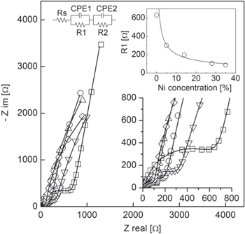
Figure 3. Nyquist plot of the complex impedance of the Ni : C nanocomposite electrodes immersed in KOH 1 M. Open squares, triangles down, circles, triangles up and rhombus refer to 0, 5, 14, 28 and 35% Ni volumetric concentrations, respectively. The electric circuit used to model the impedance data is shown in the figure together with the equivalent circuit fit (solid line). The plot of the R1 parameter versus the Ni concentration in the different Ni : C nanocomposites is reported.
Download figure:
Standard image High-resolution imageTo deepen the understanding of the impedance spectra, the electrochemical systems have been modeled by the equivalent circuit reported in the inset of figure 3. The choice of the circuit is described in detail elsewhere [14, 26]. In brief, the circuit is composed by a resistance, Rs, in series with the series connection between two R/CPE networks: Rs represents the overall resistance of the system at high frequency, R1/CPE1 accounts both for the interface current collector/active material interface and the electric transport in the nanocomposite and R2/CPE2 models the low frequency part of the spectra (below the knee frequency) related to the EDL capacitance. Equivalent circuit impedance has been used to fit the complex impedance spectra of the different Ni : C electrodes and best fit parameters are reported in table 2. Considering the equivalent circuit, ESR is equivalent to the sum of Rs and R1. However, as consequence of the shift of the spectra, Rs value of different samples is constant and, as changes in ESR coincide with changes in the R1 parameter, from this point forward we will refer to R1 and/or ESR without distinction. As reported in the inset of figure 3, R1 diminishes with increasing Ni loading moving from ca. 630 Ω in the case of the pure ns-C electrode to ca. 86 Ω for the Ni : C electrode with highest Ni concentration, with a trend roughly proportional to the inverse of the Ni volumetric concentration in the nanocomposite. This trend is consistent with the evolution of the electric conductivity of the Ni : C nanocomposite thin film deposited by SCBD [49]. The impact of Ni/NiO clusters inclusion, in terms of modification of the electrode interface area available for EDL formation, is evaluated by the analysis of the part of the complex impedance spectra below the knee frequency that, as confirmed by the α exponent (α CPE2 in table 2) close to 1 of the constant phase element used to fit this part of the spectra, is related to the capacitive behavior of the electrode. EDL capacitance (CEDL), calculated at 0.1 Hz by equation (1) (where f is the frequency and Z' is the impedance imaginary part), has been used to estimate the EDL specific volumetric density of energy Evol (equation (2), where V is the volume of the electrode soaked with the electrolyte solution), considering a maximum operating voltage (U) of 1 V in agreement with the electrochemical stability window of the electrolyte solution employed


Table 2. Best fit equivalent circuit parameters for the complex impedance spectra (figure 3) of the Ni : C nanocomposites listed in table 1. The fit parameters refer to the electric circuit reported in the inset of figure 3.
| Ni : C | Rs ( ) ) |
CPE1 (Ssα) | αCPE1 | R1 ( ) ) |
CPE2 (Ssα) | αCPE2 | R2 ( ) ) |
|---|---|---|---|---|---|---|---|
| A | 20 | 34 × 10−6 | 0.930 | 632 | 435 × 10−6 | 0.884 | 140 × 103 |
| B | 33 | 59 × 10−6 | 0.863 | 301 | 707 × 10−6 | 0.875 | 14 × 103 |
| C | 84 | 132 × 10−6 | 0.695 | 198 | 604 × 10−6 | 0.900 | 25 × 103 |
| D | 52 | 82 × 10−6 | 0.749 | 105 | 613 × 10−6 | 0.914 | 13 × 103 |
| E | 17 | 146 × 10−6 | 0.787 | 86 | 680 × 10−6 | 0.915 | 8 × 10³ |
Compared to the pure ns-C electrode Ni : C electrodes show a slightly increased Evol that does not depend on the amount of embedded Ni/NiO clusters (figure 3), meaning that the inclusion of Ni/NiO nanoparticles in the carbon matrix does not alter the electrode interfacial area available for EDL formation over a wide range of volumetric concentrations. This result suggests that the inclusion of Ni nanoparticles in the ns-C preserves the high surface area of the cluster-assembled carbon and further confirms that, as shown in figure 2, Ni : C films retain the typical ns-C structure. Specific volumetric power density, Pvol, have been calculated by equation (3) (where R1 and V are the ESR and the active material volume of the electrodes, respectively) considering a maximum operating voltage (U) of 1 V. As reported in figure 4, the improved electrical conductivity owed to the embedded nickel leads to a linear increase of the maximum Pvol delivered by the electrode upon increasing volumetric concentration of Ni/NiO clusters in the active material.

Figure 4. Specific volumetric energy, Evol (open triangles), and power, Pvol (open circles), densities of the Ni : C nanocomposite electrodes at 1 V maximum operating voltage.
Download figure:
Standard image High-resolution image3.2. Heated nanocomposites
Although no ordered sp2 structures have been observed in the Ni : C nanocomposites grown at room temperature, their formation in the nanocomposite can be promoted by post deposition thermal treatments. Ns-C structural modifications catalyzed by the embedded Ni/NiO clusters have been explored by a mild thermal treatment at 300 °C in argon atmosphere. The temperature was chosen as to produce a most gentle thermal treatment still capable to activate nickel catalyzed carbon structural transformations [26]. The HRTEM micrograph of heated Ni : C film, reported in figure 5(a), shows that thermal treated nanocomposites are rich in ordered tubular onion-like structures, consisting of concentric curved graphitic sheets, uniformly distributed across the samples. These structures are not observed in a pure ns-C film which underwent the same thermal treatment (figure 5(b)), and their formation is thus attributed to the effect of the embedded Ni/NiO clusters which catalyze the graphitization of the ns-C at temperature as low as 300 °C. Due to the difference in the densities between ns-C (0.5 g cm−3) and graphite (2.2 g cm−3), the transformation of part of the ns-C induces a mean nanocomposite thickness reduction of about the 25% (measured by AFM) which indicates the graphitization of about the 40% of ns-C. The Raman spectrum of the carbon in the heated nanocomposite (figure 6(a)) is still consistent with an short range ordered structure but it significantly differs from the spectrum of the as-deposited Ni : C film. It shows a sharper G peak which is slightly upshifted from ca. 1560 cm−1 (as deposited nanocomposite) to ca. 1570 cm−1. Moreover, D and G peaks are better resolved. This evolution is consistent with the presence of the ordered graphitic structures observed in the heated nanocomposite by means of HRTEM. The Raman contribution of these structures has been isolated by the subtraction of the Raman spectrum of the as deposited Ni : C from the spectrum of the heated sample. The difference spectrum, reported in figure 6(b), exhibits a broad Raman peak around 1360 cm−1 (the defect band, D) and a sharper peak 1580 cm−1 (the graphitic band, G) with greater intensity resembling the Raman response of closed graphitic nano-shells (carbon onions) [50–52]. By the Gaussian fit of the D and G peaks, a graphitic crystallite size of ca. 8 nm is estimated using the empirical Tuinstra–Koenig relation [46, 53].
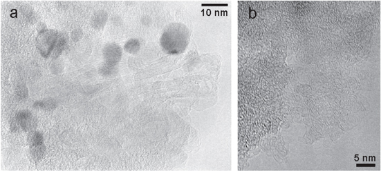
Figure 5. HRTEM micrographs of (a) Ni : C nanocomposite and (b) of pure ns-C heated at 300 °C in Ar atmosphere. The dark features in (a) are Ni-containing particles, which favor the growth of elongated, graphitic carbon structures.
Download figure:
Standard image High-resolution image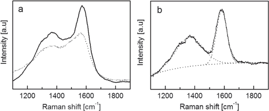
Figure 6. (a) Raman spectra of a heated (solid line) and as deposited (dotted line) Ni : C thin film (sample B in table 1). (b) Difference between the two Raman spectra of (a). The Gaussian fits of the D and G peaks in the difference spectrum are reported (dotted lines).
Download figure:
Standard image High-resolution imageThe evolution of the interfacial electrochemical properties of Ni : C nanocomposites as consequence of the formation of these onion-like carbon nanostructures, has been characterized by EIS. Nyquist plot of the complex impedance of heated Ni : C electrodes (synthesized in the same batch of the electrode studied in section 3.1) soaked in KOH 1 M as aqueous electrolyte solution is reported in figure 7 together with the response curve of the equivalent circuit reported in the figure (best fit parameters are reported in table 3). Impedance spectra have been rigidly shifted at the same real axis intercept at 0.1 MHz to accommodate the differences in the conductivity of the nickel current collector of the electrodes due to slight inhomogeneities in the sputter deposition and to allow a direct comparison between the different samples. As consequence of the heating, the high frequency arc observed in the as deposited Ni : C electrodes (figure 3) disappears and is replaced by a diagonal line with a slope of about 45°. This is reflected in the decreasing of the α exponent of the constant phase element related to the R1/CPE1 subcircuit used to fit the spectra in the frequency region above the knee frequency from ca. 0.8 (see table 2) to ca. 0.6 (see table 3) after the thermal treatment. These latter values of the CPE1 exponent indicate that the high frequency range of the spectra is characterized by a Warburg-like behavior which is consistent with the porous nature of the active material. As this part of the impedance spectrum is related both to the current collector/active material interface and to the charge transport in the electrode, this evolution suggests an enhancement both in the charge injection from the collector to the active layer and in the charge transport in the Ni : C. R1 values reported in table 3, are significantly reduced compared to the ones of the as deposited nanocomposite electrodes. This drop is consistent with the presence of the ordered graphitic structures that reasonably enhance the nanocomposite conductivity. Furthermore, after the heating, the sum of the volumetric fraction of the highly ordered graphitic carbon (roughly estimated by the decrease of the nanocomposite thickness) and of the Ni is ca. 0.16, 0.33, 0.49 and 0.51 for the samples grown with a nominal Ni concentration of 5, 14, 28 and 35%, respectively. These concentrations are near or above the percolation threshold and suggest that, besides providing additional centers for the hopping transport, graphitic sites may form, together with Ni/NiO nanoparticles, a percolative network for the charge transport inside the porous matrix. The decrease of R1 in the case of the ns-C electrode with no embedded Ni/NiO nanoparticles does not arise from a thermally induced enhancement of the electric conductivity of the carbon as no graphitization is expected in the ns-C after the thermal treatment (see figure 5(b)). The drop of R1 is thus reasonably ascribable to an enhanced electric contact at the interface between the ns-C and the Ni current collector [26]. Due to oversimplification of the equivalent circuit, we cannot disentangle the contributions of the current collector/active material interfacial contact and of the active material conductivity to the R1 parameter. The impact of the carbon graphitization on the overall porosity of the nanocomposites has been studied by the analysis of the low frequency part of their electrochemical impedance spectra that, as highlighted by the best fit equivalent circuit parameters reported in table 3, reflects the capacitive behavior of the electrodes (αCPE2 is ca. 0.9). As this range of frequency concerns with the EDL formed at the interface between the pores of the Ni : C and the KOH, it is sensitive to any changes in the nanocomposite structure induced by the heating. Figure 8 reports the EDL specific volumetric energy densities, Evol, and power densities, Pvol, of the heated Ni : C electrodes calculated at 0.1 Hz by equations (2) and (3), respectively. With the exception of the pure ns-C electrode, which structure does not change as consequence of the heating (see figure 5(b) and [26]), Evol of the thermal treated nanocomposite is about 20% higher than the one measured in the case of the as deposited samples. This enhancement indicates a modification of the specific surface area of the nanocomposites, which seems to increase and/or become more accessible for the ions of the electrolyte solution as consequence of the formation of the graphitic nanostructures. Pvol is about one order of magnitude higher compared to the one of the as deposited nanocomposite, as expected by the decrease of the overall series resistance of the electrodes (see the values of R1 in table 3). As previously discussed, the mechanism leading to the decrease of R1 and the consequent enhancement of Pvol cannot be univocally identified. It owes to the presence of ordered graphitic structures catalyzed in the ns-C not only by the embedded Ni/NiO clusters but also by the nickel current collector. While the formation of the graphitic domains in the ns-C is due to the embedded Ni/NiO clusters and proceeds only in the nanocomposites, the thermally induced graphitization of the carbon at the active material/current collector interface is common to all the electrodes contributing to the drop of the ESR also in the pure ns-C electrode [26]. We can further speculate that the disproportionately high volumetric power density exhibited by the nanocomposite with a nominal 14% Ni concentration is due to an optimal Ni : C volume ratio that maximizes the thermally induced graphitization of the ns-C.

Figure 7. Nyquist plot of the complex impedance of the heated Ni : C nanocomposite electrodes immersed in KOH 1 M. Open squares, triangles down, circles, triangles up and rhombus refer to 0, 5, 14, 28 and 35% Ni volumetric concentrations, respectively. The electric circuit used to model the interface and the equivalent circuit fit (solid line) are reported.
Download figure:
Standard image High-resolution imageTable 3. Best fit equivalent circuit parameters for the complex impedance spectra (figure 7) of the heated Ni : C nanocomposites listed in table 1. The fit parameters refer to the electric circuit reported in the inset of figure 7.
| Ni : C | Rs ( ) ) |
CPE1 (Ssα) | αCPE1 | R1 ( ) ) |
CPE2 (Ssα) | αCPE2 | R2 ( ) ) |
|---|---|---|---|---|---|---|---|
| A | 20 | 496 × 10−6 | 0.651 | 27 | 642 × 10−6 | 0.916 | 61 × 103 |
| B | 27 | 1680 × 10−6 | 0.582 | 27 | 620 × 10−6 | 0.915 | 14 × 103 |
| C | 18 | 462 × 10−6 | 0.651 | 8 | 503 × 10−6 | 0.913 | 20 × 103 |
| D | 17 | 927 × 10−6 | 0.641 | 21 | 537 × 10−6 | 0.893 | 42 × 103 |
| E | 9 | 1400 × 10−6 | 0.578 | 12 | 670 × 10−6 | 0.918 | 17 × 103 |

Figure 8. Specific volumetric energy, Evol (open triangles), and power, Pvol (open circles), densities at 1 V maximum operating voltage of the Ni : C nanocomposite electrodes heated at 300 °C in Ar atmosphere.
Download figure:
Standard image High-resolution image
4. Conclusions
The co-deposition of nickel and carbon clusters by SCBD has been demonstrated as a feasible route to synthesize porous nanocomposites with tailored and controlled electrochemical properties and fully compatible with planar microfabrication techniques. The EDL at the interface between cluster assembled Ni : C thin films and KOH 1 M have been characterized. The presence of embedded Ni/NiO nanoparticles in the carbon film preserves its high specific surface area and significantly improves the electrical conductivity of the cluster assembled carbon leading to a linearly increasing EDL specific volumetric power density with increasing Ni volumetric concentration. Embedded nickel has been shown to promote the formation of ordered graphitic nanostructures in heated nanocomposites which critically increase the rate capability of the electrodes without reducing their volumetric energy density. The inclusion of Ni in the ns-C significantly improves the low electric conductivity of ns-C based electrodes and is thus promising toward the use of ns-C based thin films as active material in electrochemical energy storage devices. Moreover by the fine control of both the amount of deposited materials and of the Ni volumetric percentage in the carbon matrix, SCBD offers the possibility of adjusting the EDL specific power and energy densities directly at the deposition stage.
Acknowledgments
Authors PP, LGB and PM gratefully acknowledge financial support from MIUR, Italian Ministry for Education, University and Research, grant number: FIRB-RBAP115AYN.