
Abstract
The strain-induced band structure change in a semiconductor can change its resistivity, known as the piezoresistive effect. If the semiconductor is also a piezoelectric material, strain-induced polarization charge can control the current transport at the metal-semiconductor contact, which is called a 'piezotronic effect'. Piezotronic effect is intertwined with piezoresistive effect in the study of present piezotronic nanowire devices. Decoupling those effects will facilitate the fundamental study on the piezotronic devices and simplify the data analysis in real applications. Here, we report a general method to separate the piezotronic and piezoresistive effects in the same nanowire, based on modified four-point measurements. Current transport characteristics of each contact was extracted and showed different responses to the strain. The piezoresistive effect was measured in zinc oxide nanowires for the first time, and the result confirmed the dominant role of piezotronic effect in the strain-induced change of transport characteristics in a piezoelectric semiconductor. This study validates the assumption made in present piezotronic devices and provides a guideline for further investigation.
Export citation and abstract BibTeX RIS
1. Introduction
The phenomenon that a mechanical strain can affect the charge carrier transport plays important roles in various fields including artificial skin [1], human-machine interface [2], strain engineering [3], etc. For a homogeneous material with electrodes, three mechanisms may alter its transport characteristics—the geometric change, the piezoresistive effect that changes the material resistivity [4], and the piezotronic effect that changes the interfacial barrier between the material and the electrode [5, 6].
Piezoresistance roots in the bending/splitting of electronic band structures under strain and is significant in semiconductors like silicon nanowires [7, 8]. Unlike piezoresistance, piezotronic effect only appears in semiconductors with a non-centrosymmetric crystal structure, such as wurtzite zinc oxide (ZnO) and gallium nitride (GaN). In those materials, piezoelectric charges control the barrier height at the metal-semiconductor interface and modulate the carrier transport [9–11]. The single crystal ZnO nanowire is the most studied piezotronic material, due to its simple synthesis [12, 13], flexibility [14], and robustness [15, 16]. Piezotronic nanowire devices demonstrate superior strain sensitivity and have wide applications in strain-gated transistors [17–19], tactile sensor array [20], logic circuits [21], memories [22], etc.
A typical piezotronic device consists of a ZnO nanowire and two metal electrodes on the ends. Consequently, the change of transport characteristics under strain combines the piezotronic effect at two contacts and the piezoresistive effect in the nanowire (the geometric influence is relatively small and can be neglected). Previous studies assumed that the piezotronic effect dominated the current transport because of the asymmetric current change at forward and reverse biases[20, 23]. However, there is no report on the piezoresistance of ZnO nanowires, and quantitative comparison of the piezotronic and piezoresistive effects is still lacking. It is essential to develop a general method which can separate those effects and reveal the strain-dependent transport characteristics of individual contacts and the nanowire itself.
2. Experimental section
Separation of the two effects is based on a multi-terminal nanowire device. We first synthesized ultra-long ZnO nanowires with diameters between 400 and 800 nm through chemical vapor deposition [24, 25], and then transferred a nanowire onto a polyethylene terephthalate(PET) substrate, as illustrated in figure 1(a). Prior to the electrodes deposition, a 200 nm SU-8 layer was spin-coated on the substrate and produced a non-conformal coverage around the nanowire, figures 1(b) and (c). The SU-8 was thicker on the two sides of the nanowire than on the top, so a short oxygen plasma ashing could expose the top part of the nanowire while the SU-8 on two sides remained, figure 1(c). The SU-8 film, called a lifting layer [26, 27], planarized the step between the nanowire and the substrate for electrodes deposition (figure 1(d)). More importantly, it could anchor the nanowire to the substrate and transfer the strain from the substrate to the nanowire during the test. The lifting layer process is self-adaptive, as the same coating and ashing parameters worked successfully for wires with different diameters. This simple technique can be applied to similar studies on flexible nanowire electronics.

Figure 1. Fabrication of the multi-terminal device with a ZnO nanowire. (a) Schematic diagram of a nanowire transferred onto a polymer substrate. (b) An SU-8 layer is spin-coated on the substrate. (c) An oxygen plasma ashing exposes the top part of the nanowire. (d) Electrodes are deposited on the exposed nanowire. (e) Scanning electron microscopy image of as-synthesized ZnO nanowires; the nanowire grows along its c-axis. (f) Atomic force microscopy image of a nanowire in the SU-8 lifting layer with the top part exposed; the inset shows a section view of the scan. (g) Optical microscopy image of a nanowire with multiple electrodes.
Download figure:
Standard image High-resolution imageThe electrodes were patterned on the ZnO nanowire with a photolithography liftoff process. It is worth noting that fully cross-linked SU-8 lifting layer is a permanent epoxy and will not be attacked by the liftoff solvent. We deposited 100 nm titanium, 200 nm copper, and 10 nm gold through evaporation. The titanium layer formed the electric contact with the nanowire, the thick copper layer improved the mechanical strength of the electrodes, and the thin gold layer prevented the electrodes oxidation. After the device fabrication, the voltage–current curves of nanowires were obtained with a current source (Keithley 6221) and a nanovoltmeter (Keithley 2182A).
3. Results and discussion
Figure 1(e) shows a scanning electron microscopy image of the as-synthesized nanowires, and figure 1(f) is an atomic force microscopy (AFM) image of a thick wire surrounded by a lifting layer on the substrate. The inset of figure 1(f) plots a cross section of the AFM scan, in which the exposed part of the wire and the two SU-8 slopes are distinguishable. The final device has a series of electrodes on a secured ZnO nanowire, figure 1(g).
Ideally, metal electrodes on a ZnO nanowire form either rectifying Schottky contact or linear Ohmic contact, solely determined by their work functions. In reality, the contact depends on the surface condition, crystallinity, and chemical reaction as well, and thus the contact can have more varieties[28]. By using titanium as the electrodes, we obtained both linear Ohmic contacts and nonlinear barrier contacts. We configured a four-point connection (figure 2(a)) to test the piezoresistance in nanowires with Ohmic contacts. The strain was applied to the nanowire by bending the substrate, as illustrated in figure 2(b). Because the nanowire stays on the surface of the substrate and its dimension is much smaller than the substrate, it has mainly tensile/compressive strain with minimal shear strain. Since the strain, current density, and electric field are all along the c-axis of the ZnO nanowire, this setup characterizes the longitudinal piezoresistive effect [29], which is the most relevant for piezotronic nanowire devices.
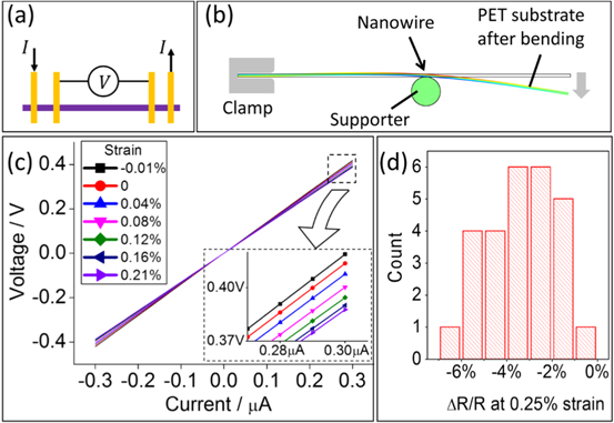
Figure 2. Measurement of the piezoresistive effect in devices with Ohmic contacts. (a) Schematic diagram of the four-point measurement. (b) Schematic diagram of the experimental setup used to stretch the ZnO nanowire; the polymer substrate is deflected by a programmable linear motor. (c) Voltage–current curves of a nanowire under different strains, obtained with the four-point configuration in (a); the inset is a zoom-in view of the curves at the high current end. (d) Histogram of the relative change of resistance, measured from 27 nanowire segments under tensile strain.
Download figure:
Standard image High-resolution imageFigure 2(c) shows typical voltage–current (V–I) curves from the four-point measurement. The resistance decreases when the nanowire is stretched, and increases when it is compressed. The histogram in figure 2(d) represents the relative change of resistance under 0.25% tensile strain among 27 nanowires. All the nanowires have lower resistance under the tensile strain, with the ΔR/R value between −0.3% and −6.8%. Since a pure geometric change increases the resistance by 0.4% at 0.25% strain, the resistivity of nanowires must have decreased here. For the first time we show that the c-orientated n-type ZnO nanowire has a negative longitudinal piezoresistive coefficient.
The variance of the ΔR/R value among nanowires can come from two factors. First, piezoresistance depends on semiconductor parameters such as the carrier concentration [30]. Based on the resistance and geometry of those ZnO nanowires, we found that the resistivity can be more than an order of magnitude different, suggesting great variance in the carrier density among nanowires. Second, the 0.25% strain is the strain on the surface of the flexible substrate. The actual strain in the nanowire depends on its diameter (discussed later) and the adhesion between the SU-8 and the nanowire, and thus can deviate to different extents from the 0.25% value.
Variation of the four-point measurement, as illustrated in figure 3(a), can introduce the contact 1 and contact 2 in addition to the nanowire resistance. At a certain current, subtracting Va from Vb gives the potential difference across contact 1 (ΔV1). Similarly, subtracting Va from Vc reveals the potential difference across contact 2 (ΔV2). When the Ti/ZnO contact has a barrier, the change of ΔV1 and ΔV2 under strain represents the piezotronic effect. Therefore, measurements in figure 3(a) can separate the piezotronic and piezoresistive effects.
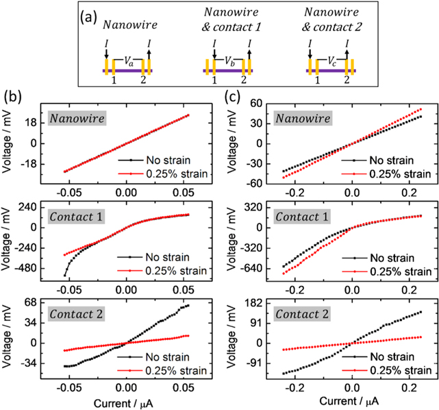
Figure 3. Comparison of the piezotronic effect and the piezoresistive effect in devices with barrier contacts. (a) Schematic diagram of three different connections to extract the nanowire resistance and two contacts. (b) Voltage–current (V–I) measurement of a typical device; the V–I curve of nanowire resistance is directly obtained, while the V–I curves of contact 1 and contact 2 are derived by subtracting Va from Vb and Vc in (a). (c) Voltage–current curves of another device obtained with the similar methods; the measured nanowire resistance increases under the tensile strain.
Download figure:
Standard image High-resolution imageFigure 3(b) compares the V–I curves of nanowire resistance, contact 1, and contact 2 in a nanowire with barrier contacts. The curves of contact 1 and contact 2 are obtained after the subtraction of Va from Vb and Vc in figure 3(a). Under the same current, much higher voltage across contact 1 and contact 2 than that across the nanowire indicates that the interfacial barriers are more significant than the nanowire resistance. More importantly, V–I curves of the two contacts have prominent change under 0.25% tensile strain while the change of nanowire resistance is negligible. Thus the piezotronic effect at the contacts is much greater than the piezoresistive effect in the nanowire, which supports directly the assumption made in previous studies [6].
Moreover, decoupling the piezotronic effects at the two contacts enables us to extract detailed information at the individual contact. Figure 3(b) shows that contact 1 behaves as a rectifying barrier under zero strain, and the tensile strain lowers the barrier and increases the reverse current. Contact 2 has a lower barrier height than contact 1 and is close to an Ohmic contact, suggesting that the tunneling may dominate the current transport [31]. The strain further reduces the barrier height. In terms of strain sensing, contact 2 has higher sensitivity than contact 1. Such distinctive transport characteristic of contact 1 and contact 2, when lumped in a two-terminal device, complicates the analysis and makes it challenging to predict the device behavior. In fact, most ZnO piezotronic devices in the literature formed different electric contacts at two ends even with the same metal, so it is necessary to analyze the two contacts independently.
Figure 3(c) shows the V–I curves of another multi-terminal device. While the piezotronic effect still dominates, this nanowire has an unusual piezoresistive effect. The tensile strain increases nanowire resistance with ΔR/R as high as 23%. The positive piezoresistive coefficient opposes the result in figure 2(d) where all the nanowires with Ohmic contacts have a negative coefficient. Such a phenomenon has been observed in several devices with barrier contacts, and here we propose a possible explanation. Although the four-point measurement excludes the contacts, the effect of contacts can extend into the thin nanowire. Numerical calculation shows that when ZnO nanowire forms Schottky contacts with electrodes, the region near the contact has a lower carrier density than the rest part of the nanowire. Strain-induced polarization charge at the contact further changes the carrier distribution [10]. Therefore, a strain could alter the carrier profile within the nanowire, which in turn affects the overall resistance. The measured piezoresistive effect depends on the contacts, and it may be more properly called an 'apparent' piezoresistive effect.
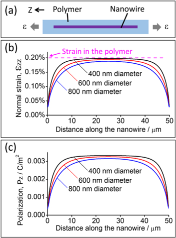
Finally, we discuss a feature of the multi-terminal piezotronic device, i.e., the electrodes are on the side surface of the nanowire instead of its two ends. The piezotronic effect is caused by the polarization charge [10, 11]. For a ZnO nanowire under uniform tensile/compressive strain, the charge only appears at the two ends. Here, the piezotronic effect with the electrode on the side surface is ascribed to the non-uniform strain along the nanowire. We used COMSOL Multiphysics to simulate the elastic and piezoelectric behavior of a ZnO nanowire embedded in a polymer matrix. For simplicity, we assume ZnO is an insulator and there is no slipping between the nanowire and the polymer. Two ends of the polymer are subject to uniform tensile loads, as shown in figure 4(a), and the strain is transferred from the polymer to the nanowire. Figure 4(b) shows the normal strain along the central axis of nanowires with different diameters. The strain near the two ends of the nanowire is much lower than that in the polymer far away from the nanowire (indicated by the dashed line). As the diameter becomes larger, the average strain in the nanowire is lower. The strain distribution results from the difference between the elastic moduli of the ZnO and the polymer. Figure 4(c) shows the electric polarization along the central axis of the nanowires, which has the similar characteristics as the normal strain. By calculating the divergence of the polarization field, we found that the polarization charge density is the highest at the two ends, but non-zero on the side surface. Positive charge appears near the (0001) end of the nanowire, and the charge density decays further away from the end surface. The (000 ) end has a similar distribution of negative charge.
Figure 4. Simulation of the non-uniform strain in ZnO nanowires. (a) Schematic diagram of a nanowire embedded in a polymer matrix. (b) Normal strain along the central axis of nanowires with the same length but different diameters; the dashed line indicates the normal strain in the polymer far away from the nanowire. (c) Electric polarization along the central axis of nanowires with the same length but different diameters.
Download figure:
Standard image High-resolution image
The charge distribution from the ends to the middle of the nanowire can produce a rich variety of piezotronic effects, depending on the positions of the electrodes. When the charges near the two electrodes have the same polarity, piezotronic effects raise or reduce the barrier height of both electrodes, e.g., the device in figure 3(b). If the charges have different polarities, the piezotronic effects are opposite at the two contacts, such as the device in figure 3(c). When the electrodes are in the region where the polarization charge is negligible and the change of the barrier height is insignificant, the device will not show significant piezotronic effects. If the strain distribution can be under good control, it is not only feasible but also beneficial to put contacts on the side surface of a nanowire, in order to have multiple piezotronic effects with desired properties.
4. Conclusions
The objective of this work is to independently study the piezotronic effect and the piezoresistive effect in a ZnO nanowire. With a four-point connection, we extracted the piezoresistive effect in ZnO nanowires for the first time and found that a tensile strain reduces the resistivity. However, a barrier contact could influence the apparent piezoresistive effect even with the four-point connection. Modified four-point measurements revealed the piezotronic effect at a barrier contact, which proves to be more significant than the piezoresistive effect. In addition, the feasibility and advantage of using piezotronic effects on the side surface of nanowires has been discussed. The general methods developed in this work contribute to the fundamental understanding of the piezotronic effect and provide guideline for the practical applications.
Acknowledgments
The authors are truly grateful for the financial support from the Department of Mechanical Engineering and the College of Science and Engineering of the University of Minnesota. Research is also supported by NSF (ECCS-1150147). The electron microscopy image was obtained in the Characterization Facility, University of Minnesota, which receives partial support from NSF through the MRSEC program. The device fabrication was performed in the Minnesota Nano Center, a part of NSF-funded National Nanotechnology Infrastructure Network.