Abstract
In this paper, the structural and electrical modifications induced, in the nanoscale, by a rapid thermal oxidation process on AlGaN/GaN heterostructures, are investigated. A local rapid oxidation (900 ° C in O2, 10 min) localized under the anode region of an AlGaN/GaN diode enabled a reduction of the leakage current with respect to a standard Schottky contact. The insulating properties of the near-surface oxidized layer were probed by a nanoscale electrical characterization using scanning probe microscopy techniques. The structural characterization indicated the formation of a thin uniform oxide layer on the surface, with preferential oxidation paths along V-shaped defects penetrating through the AlGaN/GaN interface. The oxidation process resulted in an expansion of the lattice parameters due to the incorporation of oxygen atoms, accompanied by an increase of the crystal mosaicity. As a consequence, a decrease of the sheet carrier density of the two-dimensional electron gas and a positive shift of the threshold voltage are observed. The results provide useful insights for a possible future integration of rapid oxidation processes during GaN device fabrication.
Export citation and abstract BibTeX RIS
1. Introduction
Gallium nitride (GaN) and related Al-based alloys (AlxGa1−x N) have outstanding physical properties, making them promising materials for high power and high frequency electronic devices [1]. In particular, owing to the high-breakdown field of the material [2] and to the presence of the two-dimensional electron gas (2DEG) [3], AlGaN/GaN heterostructures make it possible to fabricate high electron mobility transistors (HEMTs) operating up to several gigahertz at power densities of several W mm−1 [4].
Typically, AlGaN/GaN HEMTs are 'enhancement mode' devices driven by a negative bias applied to a Schottky gate. However, a Schottky gate contact can have a high reverse leakage current, limiting the off-state performance of the device. Hence, to overcome this limitation it is advantageous to employ metal–insulator–semiconductor HEMTs (MIS-HEMTs or MOS-HEMTs), i.e. depositing a dielectric film below the gate electrode [5–9].
Besides the dielectric deposition, also the direct oxidation of AlGaN/GaN heterostructures has attracted considerable interest in the last few years, due to the possible implementation in GaN device technology. Firstly, Masato et al [10] proposed selective local thermal oxidation for device isolation in AlGaN/GaN HEMTs, as an alternative approach to the mesa etching or ion-implantation. Lately, we have reported that a long oxidation process can produce 2DEG isolation in AlGaN/GaN heterostructures even though the thickness of the surface oxide does not reach the depth of the 2DEG [11, 12]. More recently, rapid thermal oxidation processes were proposed as simple methods to passivate the surface of GaN-based HEMTs and to reduce the leakage current [13–15]. In this context, novel cost-effective oxidizing techniques, e.g. ozone- or hydrogen-peroxide-based treatments have also been reported to improve the HEMT performances [16, 17].
Since the incorporation of impurities during GaN growth (e.g. oxygen, magnesium, etc) can induce nanoscale changes of the lattice parameters of the material [18, 19], correlating the structural and electrical modification caused by rapid oxidation in AlGaN/GaN heterostructures deserves further attention, due to the possible implications for HEMT technology. However, this specific aspect has not been addressed in detail in the previous literature. In this context, material defects, such as the so-called 'V-defects', can have a role during the oxidation process, those defects, largely present in nitride heterostructures at the end of dislocations, can be detrimental for the 2DEG mobility behavior [20–24].
This paper reports on the nanoscale electrical and structural modification of the properties of AlGaN/GaN heterostructures grown on Si(111), induced by rapid thermal oxidation at 900 ° C. The combination of several analytical techniques and the study of the electrical behavior of MIS diodes provided a more comprehensive scenario of the effects induced by this rapid oxidizing annealing.
With respect to our previous investigations focusing on the 2DEG insulation in AlGaN/GaN HEMTs [11, 12], in the present work the annealing time has been significantly reduced in order to explore the possibility of using the process in MOS-HEMT technology. Indeed, the reported results could be useful in device engineering to establish the potentialities and the limits of integration of such processes. The impact of material defects, typically present in heterostructures grown on Si substrates, is also highlighted.
2. Experimental details
Al0.27Ga0.73N/GaN heterostructures were grown by metal organic chemical vapor deposition (MOCVD) on Si(111) substrates with an AlN buffer layer, using trimethylgallium (TEGa) and ammonia (NH3). The thickness of the AlGaN barrier layer was 25 nm, while that of the underlying GaN was 0.8 μm. The nominal sheet carrier concentration and mobility were 1 × 1013 cm−2 and 1080 cm2 V−1 s−1, respectively. On these samples, test-diodes were fabricated in order to monitor the effect of a rapid local thermal oxidation on the electrical properties of the heterostructure. First, the sample was patterned with a thick SiO2 hard mask and a local oxidation has been performed by a rapid (10 min) annealing process in O2 at 900 ° C. After removing the hard mask, a thin (∼5 nm) SiO2 layer was deposited on the surface by plasma enhanced chemical vapor deposition to protect the oxidized region during the following fabrication steps. Afterwards, this layer was defined by wet etching to cover both the thermally oxidized and some non-oxidized AlGaN regions. With this procedure, three types of test-diodes with a Pt/Au bilayer Schottky contact [25] were fabricated: (1) conventional diodes without any insulator under the Schottky contact ('reference'); (2) diodes with the local thermal oxide and the protective deposited SiO2 below the Schottky contact ('MIS thermal'); (3) diodes only with the deposited SiO2 below the Schottky contact ('MIS deposited'). The ohmic contacts for these devices were formed by an annealed Ti/Al/Ni/Au stack [26], deposited on the AlGaN barrier layer, i.e. in a region that was protected by the thick SiO2 hard mask during the thermal process in O2. It is important to point out that the three types of devices were fabricated all on the same wafer.
The electrical properties of the diodes were monitored by current–voltage (I–V) and capacitance–voltage (C–V) measurements, acquired on a Karl Suss probe station equipped with a parameter analyzer.
The nanoscale morphological and electrical modifications induced by the oxidation on the AlGaN surface were investigated by atomic force microscopy (AFM) and conductive-AFM (C-AFM). A similar nanoscale approach was recently adopted by Fontserè et al [27] to study the properties of metal/AlGaN/GaN HEMT devices.
Structural analyses were carried out on blanket samples to monitor the modification of the crystalline quality induced by the oxidation process. In particular, cross-section transmission electron microscopy (TEM) was performed using a 200 kV JEM 2010 JEOL microscope. Moreover, in-plane and out-of-plane x-ray diffraction (XRD) analyses were done using a high resolution x-ray diffractometer (D8Discover Bruker AXS), equipped with a Cu-Kα source, a Göbel mirror, and Ge monochromators which guarantee an angular resolution of 0.002°.
3. Results and discussion
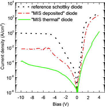
Firstly, current–voltage (I–V) characterization of the test-diodes was performed to investigate the effects of the rapid local oxidation below a metal gate and the impact on the overall electrical behavior of the heterostructures. Figure 1 shows the I–V characteristics of the devices. The forward part of the I–V curves in the three diodes clearly exhibit a large ideality factor n. In fact, by using the thermionic emission model, an increase of n from 2.13 to 3.16 is obtained from the 'reference' to the 'MIS deposited' diode, while a similar value of the Schottky barrier was determined (∼0.9 eV). On the other hand, even stronger non-ideal behavior (n = 4.99) is observed for the 'MIS thermal' diode, which is accompanied by a reduction of the forward current. From the reverse I–V characteristics, a severe reduction of the leakage current is observed in the 'MIS thermal' diode, which integrates both the thermal oxide and the deposited protective oxide below the Schottky contact, with respect to the 'reference' and 'MIS deposited' diodes. As an example, at a reverse bias of −5 V the leakage current density of the 'MIS thermal' diode was 10−5 A cm−2, i.e. three orders of magnitude lower than that of the 'MIS deposited' and even five orders of magnitude lower than in the 'reference'. The Schottky barrier enhancement and leakage reduction observed under our conditions is much more pronounced than those preliminarily reported after oxidizing treatments at lower temperatures (500 ° C) [28]. Here, it is important to point out that the electrical properties of the material in the non-oxidized regions were not significantly degraded by the thermal budget itself, in contrast to what was observed after long (900 ° C, 12 h) runs [12]. In fact, by using the transmission line model (TLM) structures it was verified that the sheet resistance of the material outside the oxidized regions remained almost unchanged after the 10 min process at 900 ° C with respect to its initial value (RSH = 577 ± 5 Ω/□).
Figure 1. Forward and reverse I–V characteristics of the three devices: 'reference' (black dashed line), 'MIS deposited' (red dash-dotted line), and 'MIS thermal' (green continuous line) diode.
Download figure:
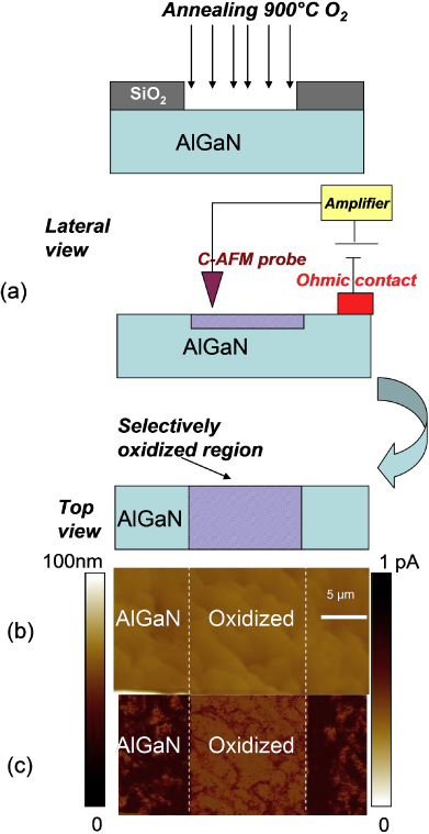
Standard image High-resolution imageNanoscale electrical characterization by C-AFM has been employed to probe locally both the AlGaN bare surface and the oxidized region. To perform these measurements, appropriate test patterns were created by optical lithography. In particular, by patterning a thick SiO2 hard mask, it was possible to define selectively oxidized regions adjacent to non-oxidized areas. The hard mask was removed by wet etching prior to AFM and C-AFM measurements. A schematic of the sample preparation and experimental setup is depicted in figure 2(a). The color scales in the current maps acquired by C-AFM were set in order to emphasize the contrast between these adjacent regions.
Figure 2. (a) Schematic of the sample preparation and experimental setup for AFM and C-AFM measurements. (b) Surface morphology and (c) current map, determined by AFM and C-AFM in non-oxidized (AlGaN) and oxidized regions of the sample surface.
Download figure:
Standard image High-resolution imageFigures 2(b) and (c) show the nanoscale morphological and electrical analysis performed by AFM and C-AFM on the patterned sample. The current maps were acquired in lateral configuration [29], by applying a bias of −2 V between the ohmic contact fabricated on the AlGaN surface and the conductive diamond tip of the AFM.
As can be seen, the morphology of the non-oxidized AlGaN region is almost indistinguishable from that of the oxidized areas (figure 2(b)), thus indicating that the performed oxidation process did not lead to substantial changes in the surface roughness. On the other hand, a clear difference is visible in the C-AFM current map (figure 2(c)) that shows an electrical contrast corresponding to the locally oxidized patterns created on the sample surface. This is due to the fact that the current flowing through the oxidized AlGaN areas (brighter region) is almost two orders of magnitude lower than the current flowing through the non-oxidized AlGaN surface (darker regions). The result demonstrates that the oxidized layer has an insulating behavior with respect to the surrounding non-oxidized AlGaN.
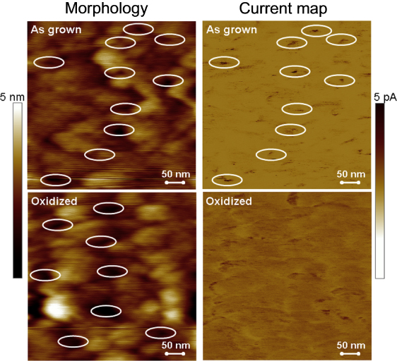
To better visualize the changes of the surface properties at the nanoscale, the AFM and C-AFM scans were also acquired on a 500 × 500 nm2 area (see figure 3), both on the as-grown and on the oxidized sample. As can be seen in figure 3, using this scan area, the morphological images show the presence of defects (depressions) on the sample surface of both the as-grown and the oxidized sample (highlighted by the white circles). From the AFM images, the density of these surface defects was estimated to be in the order of 3–4 × 109 cm−2, in both samples. In the as-grown sample, these morphological surface defects are clearly correlated with high current conductive spots (white circles) observed in the current map acquired under a forward bias of +1 V to the tip. On the other hand, no conductive spots are visible in the current map of the oxidized sample. Hence, it can be concluded that these near-surface defects are preferential conductive paths for the leakage current, and they are almost completely passivated by the oxidation process.
Figure 3. Surface morphology (left) and current maps (right) of the as-grown sample and oxidized sample. The white circles are shown to indicate the morphological surface defects and the corresponding current spots (in the as-grown sample).
Download figure:
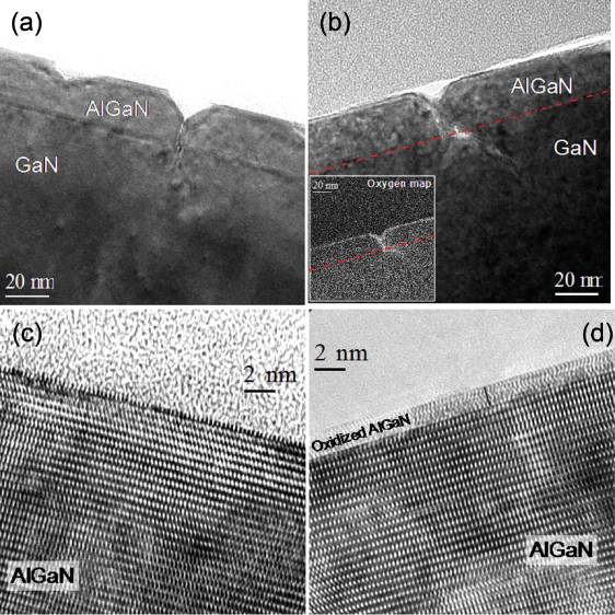
Standard image High-resolution imageIn order to clarify the nature of these defects and their eventual role in the oxidation process on the overall sample microstructure, cross-section TEM and HRXRD analyses were performed on the samples. Figure 4 reports the cross-section TEM micrographs of the samples before and after thermal oxidation. This analysis clarified the nature of the surface morphological defects observed by AFM. In fact, as can be seen in the near-surface region of the as-grown sample, i.e. in the upper part of the AlGaN barrier layer, V-shaped defects are present. These V-defects are pits localized at the end of dislocations passing through the AlGaN/GaN interface. The high density of V-defects in AlGaN/GaN heterostructures grown on Si can be prevented by the use of AlN spacers at the AlGaN/GaN interfaces [24], which, however, were not present in our samples. In spite of the presence of those defects, a very flat AlGaN/GaN interface is observed in the as-grown sample, as can also be seen by the high resolution TEM image in figure 4. After rapid thermal oxidation at 900 ° C a uniform and conformal (1.5 nm-thick) oxide layer is formed at the AlGaN surface. Considering that an oxidation rate of 1.2 nm h−1 has been estimated for longer annealing times at the same temperature [12], the measured thickness suggests the occurrence of a nonlinear oxide growth rate. While the high resolution TEM image (figure 4(d)) suggests the formation of a crystalline oxide, it was not possible to unambiguously identify the composition of this layer due to its extremely small thickness. However, according to previous oxidation experiments performed on AlGaN samples with a similar Al content (27%) [30–32], it is reasonable to assume that the oxidized layer is composed of both Al2O3 and Ga2O3 phases.
Figure 4. (Top) Cross-section TEM analysis of the as-grown (a) and of the oxidized sample (b). The inset shows the oxygen chemical map in the proximity of a V-defect. (Bottom) High resolution TEM images of the AlGaN layer for the two samples ((c) and (d)).
Download figure:
Standard image High-resolution imageIt is interesting to point out that the oxide layer covers in a conformal manner also the sidewalls of the V-defects sidewalls. The use of energy filtered transmission electron microscopy (EFTEM) [33] enabled us to get further information on the penetration of the oxygen atoms inside the AlGaN layer. In particular, the chemical map of oxygen determined by EFTEM (shown in the inset of figure 4(b)) revealed the preferential diffusion of oxygen through the V-defects down to the GaN buffer layer. Additionally, the AlGaN/GaN interface was found to be locally modified (with respect to the as deposited layer) by the annealing, since extended defects in the GaN substrate close to the AlGaN/GaN interface and embedded between two contiguous V-defects, were found (in figure 4(b) the AlGaN/GaN interface is indicated by a dashed line).
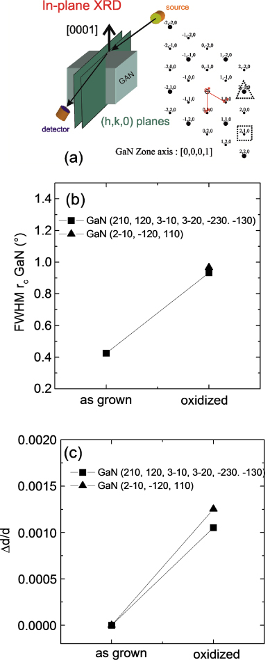
Complementary information on the structural modification induced by the rapid oxidation in terms of crystal quality (i.e. mosaicity, lattice parameters, etc) was provided by HRXRD analyses in in-plane geometry, using an incident angle such that the penetration depth in the entire structure was of ∼100 nm. The investigated area has a diameter of ∼3 mm. In this configuration, crystallographic planes perpendicular to the sample surface, thus having (h,k,0)-type Miller indices, can be investigated, as indicated in the schematic of figure 5(a). In particular, planes having large reciprocal space vectors were chosen (see the dashed square and triangles in figure 5(a)) in order to improve the angular resolution. The full width at half maximum (FWHM) of the rocking curves of the (2, − 1,0) and (2,1,0) GaN planes-family is reported in figure 5(b), for the as-grown material and for the material subjected to rapid annealing in O2 at 900 ° C. It has been observed that the FWHM increases from 0.42° to 0.93° by annealing the sample in oxygen ambient. This behavior indicates a significant increase of the mosaicity of film along the a–b plane of the hexagonal GaN structure. This finding, in turn, is consistent with the local AlGaN/GaN interface degradation observed in some regions of the TEM slice.
Figure 5. (a) Schematic of the in-plane x-ray diffraction configuration and (0001) GaN zone axis; (b) GaN FWHM of the rocking curves related to the (2, − 1,0)- and (2,1,0)-type crystallographic planes, both for the as-grown and for the oxidized sample; (c) interplanar distance for the same planes.
Download figure:
Standard image High-resolution imageFigure 5(c) shows the interplanar distance of those crystallographic planes. An increase of the interplanar distance by ∼0.12% was systematically measured by the shift of the Bragg peaks. The result can be explained by the occurrence of oxygen diffusion into the GaN lattice through the V-defects. In fact, it has been reported that the incorporation of impurity atoms in GaN can lead to modification of the lattice parameters, both due to a size effect (associated to the relaxation of host atoms around the impurity), and also to a deformation-potential effect (since the impurity can promote free carriers either in the conduction or valence band) [34]. According to this description, the relative variation of the lattice parameter induced by the incorporation of impurities is associated to two parameters βsize and βe,h [34], through the relation

where NO is the oxygen concentration in cm−3.
Inserting in equation (1) the experimentally observed increase of the lattice parameter (0.12%), and the values of the parameters βsize and βe,h for oxygen [34], it was possible to estimate an oxygen concentration incorporated in GaN of 4.8 × 10²⁰ at cm−3. This can be a reasonable value in the presence of material defects acting as preferential diffusion paths for the oxygen atoms present in the annealing atmosphere [35]. In fact, assuming the relationship for oxygen diffusion in GaN reported in [35], for our annealing temperature of 900 ° C a diffusion coefficient D(O2,900 °C) = 4.63 × 10⁻¹³ cm2 s−1 was calculated. Hence, for an annealing time of 10 min (t = 600 s), we could estimate a diffusion length  of ∼170 nm, which is comparable with the typical distance between dislocations found by TEM analysis in our material.
In this context, it is worth noting that similar samples annealed in neutral atmosphere (Ar) at the same thermal budget showed only very small changes in the lattice parameter with respect to the annealing in oxygen (XRD not shown). This result confirms the role of the annealing ambient on the microstructural modification of GaN layers subjected to thermal budgets [36].
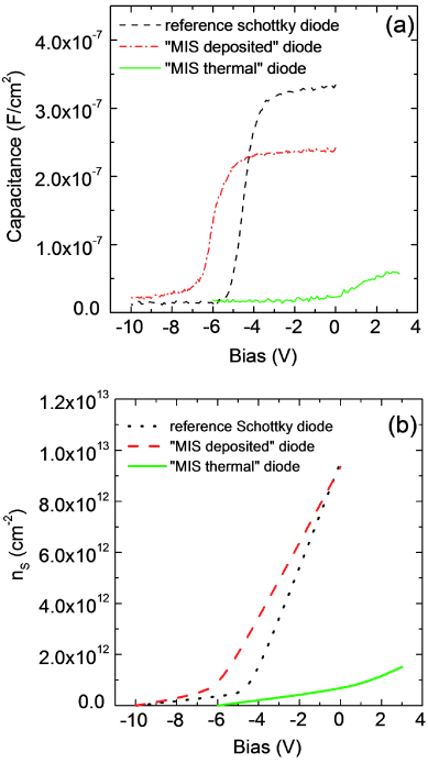
C–V analyses of the diodes have been performed to quantify the effects of the structural modification on the electrical properties of the heterostructure. As can be seen in figure 6(a), a decrease of the accumulation capacitance (from 3.34 × 10⁻⁷ to 2.42 × 10⁻⁷ F cm−2) is observed from the 'reference' to the 'MIS deposited' device, due to the presence of the insulating SiO2 layer. As can be seen, in the 'MIS deposited' diode the transition from accumulation to 2DEG depletion takes place at a more negative bias, as expected for a MIS structure since part of the applied gate bias drops on the dielectric. However, this trend is not observed in the 'MIS thermal' diode. In fact, in this case the transition from accumulation to depletion in the C–V curves is scarcely visible, and it occurs at more positive bias values, being the maximum saturation capacitance (5.9 × 10⁻⁸ F cm−2) significantly reduced with respect to the other devices. The strong reduction of the capacitance in the thermally oxidized structure indicates a local depletion of the charge in the 2DEG.
Figure 6. (a) C–V characteristics of the three devices: 'reference' (black dashed line), 'MIS deposited' (red dash-dotted line), and 'MIS thermal' (green continuous line) diode. (b) Sheet carrier density nS as a function of the gate bias Vg for the same devices.
Download figure:
Standard image High-resolution imageTo be more quantitative about the effects of the rapid local oxidation on the 2DEG properties, the sheet carrier concentration nS in the heterostructure was extracted by integrating the C–V curves over the entire range of the applied gate bias Vg [3]:

where q is the electron charge and A is the device area.
In figure 6(b), the values of nS are reported as a function of the gate bias Vg for the three devices. As can be seen, while the values of nS of the 'reference' and of the 'MIS deposited' are almost comparable (9.35 × 1012 cm−2), a significant decrease of nS occurred in the 'MIS thermal' device (9.1 × 1011 cm−2). The value of the threshold voltage Vth can be estimated as the intercept on the Vg axis from a linear fit of the curves. While the 'reference' diode has Vth =− 4.69 V, the values of Vth in the 'MIS deposited' and in the 'MIS thermal' diodes were −6.39 V and −1.26 V, respectively. The positive shift of Vth observed in the 'MIS thermal' diode with respect to the 'MIS deposited' is fully consistent with the experimentally observed reduction of nS from 9.35 × 10¹² to 6.87 × 1011 cm−2 upon rapid oxidation.
In spite of the strong reduction of the 2DEG density, the fact that the properties of the 2DEG in the non-oxidized regions (i.e. on the same wafer) remained almost unchanged suggests the possibility of integrating such a process in the gate recessed region of MOS-HEMT structures.
4. Conclusion
This paper reported on the nanoscale electrical and structural modification of the properties of AlGaN/GaN heterostructures subjected to rapid thermal oxidation at 900 ° C. Although the formation of a thin oxidized layer allows electrically passivating surface defects, thus reducing the leakage current in MIS diodes, significant structural and electrical modifications of the system were observed.
In particular, a preferential oxygen in-diffusion throughout material defects at 900 ° C led to an increase of the mosaicity and also to an expansion of the lattice parameters by 0.12% in the GaN layer at least to a depth of 100 nm, as deduced by in-plane HRXRD analyses. From these data, the oxygen incorporation was estimated to be in the order of a few at.%. In addition, these structural modifications resulted in a decrease of the sheet carrier concentration of the 2DEG (from 9.35 × 10¹² to 6.87 × 1011 cm−2) and a positive shift of the threshold voltage.
Based on these results, we believe that a controlled oxidation can be used to achieve a systematic positive shift of the pinch-off bias, with a limited effect on the 2DEG properties. Hence, this process deserves still further scientific investigation with the aim to integrate it in normally off HEMT technology and/or hybrid MOS-HEMT devices.
Acknowledgments
The authors would like to thank Corrado Bongiorno for his valuable contribution during TEM analysis, and Salvatore Di Franco for sample processing. This work was partially supported by the national project PON Ambition Power (PON01_00700).

