
Abstract
We report for the first time a novel room temperature methane (CH4) sensor fabricated using porous tin oxide (SnO2) nanorods as the sensing material. The porous SnO2 nanorods were synthesized by using multiwall carbon nanotubes (MWCNTs) as templates. Current versus time curves were obtained demonstrating the room temperature sensing capabilities of the sensor system when exposed to 0.25% CH4 in air. The sensor also exhibited a wide temperature range for different concentrations of CH4 (25–500 °C), making it useful in harsh environments as well.
Export citation and abstract BibTeX RIS
1. Introduction
Chemical sensors are used in a wide variety of applications, such as environmental monitoring, fire detection, emission monitoring, and health monitoring [1, 2]. The fabrication of chemical sensors involving nanostructured materials holds the potential for the development of sensor systems with unique properties and improved performance. Semiconducting metal oxides such as tin oxide (SnO2) have been shown to respond to relevant chemical species such as oxygen (O2), carbon monoxide (CO), ethanol (C2H5OH), nitric oxides (NOx), propylene (C3H6), and hydrogen (H2) [3–6]. There are a number of advantages to improving the capabilities of sensor materials such as metal oxides. For example, gas sensors based on polycrystalline tin oxide offer many advantages over current technologies for detecting reducing gases, such as low cost, long lifetime, and high selectivity and sensitivity. The sensing mechanism in semiconducting metal oxides relies on perturbations in surface conductivity induced by chemical reactions between target gases and oxygen species adsorbed onto the surface. For n-type semiconductors such as SnO2, the adsorption of oxygen creates surface-acceptor sites that immobilize conduction band electrons from the near surface region creating a depletion layer, as shown in figure 1(a). Reducing gases such as CO remove surface bound oxygen atoms, releasing the immobilized electrons, thereby decreasing the thickness of the depletion layer and hence increasing its conductivity (figure 1(b)). In contrast, oxidizing gases (e.g. NO2) further immobilize the conduction band electrons from the near surface region by creating additional surface-acceptor sites. This increases the thickness of the depletion layer, and consequently the conductivity decreases (resistance increases) [7].
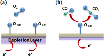
Figure 1. Schematic representation of the reactions occurring at the surface of an n-type semiconductor metal oxide. (a) Adsorption of oxygen at the surface creates surface-acceptor sites that immobilize conduction band electrons from the near surface region, creating a depletion layer. (b) Reducing gases, such as CO, remove surface bound oxygen atoms, releasing the immobilized electrons, reducing the thickness of the depletion layer.
Download figure:
Standard imageMoreover, it has been shown that the sensitivity of the sensing layer increases with decreasing grain size, therefore nanocrystalline SnO2 is expected to exhibit high sensitivity [8]. However, the processing and fabrication of nanostructures for sensor applications currently is limited in the ability to control the structural and morphological properties [9]. In addition, one of the main drawbacks of SnO2-based sensors is their high working temperature; the optimum operating temperature is usually 350–450 °C [10]. In general, a major emphasis is to produce sensors which are small in size, easy to batch fabricate and low in cost, and have low power consumption. This includes a drive to decrease the operational temperature of existing gas sensor systems to allow lower temperature operation as well as increased sensitivity and selectivity.
One important example is the sensitive detection of methane, which is a colorless and odorless flammable gas that occurs abundantly in nature as the chief constituent of natural gas. Methane gas is highly volatile and when mixed with air can cause explosions at higher concentrations due to its ready flammability. Thus, the development of a reliable and cost effective methane gas sensor remains a promising problem for timely detection of its conspicuous presence in the environment around us. However, detection of methane at room temperature is a particular difficult challenge because it is a very stable molecule. Efforts have been made to detect methane at room temperature using material systems such as single walled carbon nanotubes and MWCNTs loaded with palladium (Pd) [11, 12], and a Batron phosphorus–silicon microsensor [13], but they lack the temperature range and durability of materials such as metal oxides or metals.
A room temperature methane microsensor based on porous SnO2 nanorods has been developed. The fabrication of the microsensor includes four major steps: (1) synthesis of the porous metal or metal oxide nanorods using a sacrificial template; (2) deposition of the electrodes onto the alumina substrate; (3) alignment of the nanotubes between the electrodes and (4) deposition of the top electrodes to bury the aligned nanostructures. The sensor was operated at room temperature and detection of 0.25% methane in air was demonstrated, which is, to our knowledge, the first system of this type to use SnO2. Furthermore, the uniqueness of this porous SnO2 nanorod sensor relies on the fact that it has a wide operating temperature range (25–500 °C) for CH4 detection (2500–125 ppm), in contrast with the other material systems described above.
2. Experimental details
2.1. Electron microscopy
Transmission electron microscopy (TEM) was performed with the lanthanum hexaboride Philips CM200 microscope operated at 200 keV, equipped with a Veleta camera and a Gatan imaging filter (GIF) used for HRTEM. SEM work was done with a Hitachi S4700 instrument operated at 1 keV.
Electron energy-loss spectroscopy (EELS) was performed with the GIF in diffraction mode, with a collection semi-angle of ∼3 mrad and a TEM acceleration voltage of 200 keV. All the data were corrected by the Fourier-ratio deconvolution method [14].
2.2. Synthesis of the porous SnO2 nanorods
Porous SnO2 nanorods were synthesized using MWCNTs as templates. First, 1.0 g of MWCNTs (NanoLab) was refluxed in 100 ml of 7.0 M HNO3 for 12 h at 120 °C to remove any impurities from the nanotubes and to create oxygen-containing functional groups on the nanotube surface that act as sites for the subsequent SnO2 coating. 1.0 g of SnCl2⋅2H2O was dissolved in 40 ml of deionized water and 0.25 ml of 38% HCl was added. Next, 10 mg of the purified MWCNTs was added and the solution was sonicated for 20 min. Afterwards, the solution was stirred at room temperature for 2 h and then rinsed with deionized water until the solution was neutral. At this point, SnO2–MWCNT hybrid nanostructures are obtained [15, 16]. Sometimes MWCNTs are bundled together and are covered with the SnO2 nanoparticles, as can be seen in figure 2(a). The hybrid nanostructures are calcined at 350 °C for 3 h and then heated at 700 °C for 5 min to burn off the MWCNTs. Figure 2(b) shows a TEM image of a porous SnO2 nanorod. The mass of nanorods recovered after the final burnout step is around 8 mg. The inset of figure 2(b) is the corresponding electron diffraction (ED) pattern of the porous SnO2 nanorods. Figure 2(c) is a high resolution transmission electron microscope (HRTEM) image of the nanocrystals in the porous SnO2 nanorod.
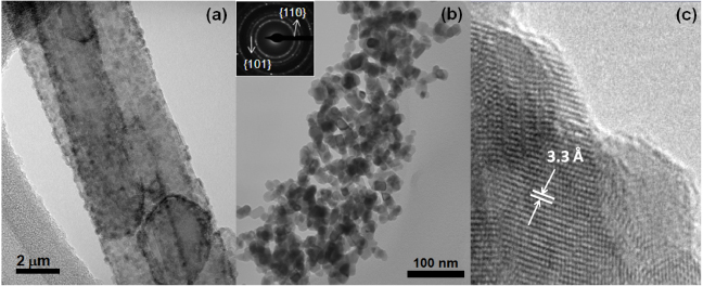
Figure 2. (a) TEM image of MWCNTs covered with SnO2 nanoparticles. (b) TEM image of a porous SnO2 nanorod. The inset shows the electron diffraction pattern. (c) HRTEM image showing that the lattice spacing corresponds to the rutile structure of SnO2.
Download figure:
Standard image2.3. Synthesis of the SnO2 nanobelts
SnO2 nanobelts were used for comparison with the porous SnO2 nanorods as a sensing material. The synthesis of the SnO2 nanobelts is described elsewhere [17]. Briefly, the nanobelts were synthesized by a thermal evaporation–condensation (TEC) approach beginning with evaporating SnO from an alumina growth boat. A tube furnace was heated to 950 °C with a small argon flow plus 5% oxygen. Without the presence of a catalyst, growth proceeds by a self-catalyzed vapor–solid mechanism with the feed boat providing heteroepitaxial nucleation sites.
2.4. Sensor fabrication and alignment of the nanostructures
After obtaining the porous SnO2 nanorods, the challenge is to integrate the nanostructures into a micro/macro sensor. Usually doing this involves repeatability issues as well as poor control of the density of the nanomaterial [18–20]. The basic ability to control the orientation and alignment of nanostructures on microstructures is still in an early stage of development, although various groups have made significant progress on a range of materials [21–25]. In our case, this has been overcome by fabricating the sensors using standard microfabrication techniques combined with the alignment of the nanostructures using dielectrophoresis (DEP). Details have been published elsewhere [17]. Briefly, alumina substrates were patterned with a sawtooth electrode pattern with contact pads through photolithography and 2500 Å of platinum was deposited by sputter deposition. The porous SnO2 nanotubes are added to a photoresist solution which is coated onto the substrate with the patterned electrodes. Dielectrophoresis is then used by applying an alternating current (ac), with a frequency of 10 MHz and 10 V peak to peak, through the contact pads in the substrate to align the porous SnO2 nanorods between the sawtooth patterned electrodes. Afterwards, a top platinum electrode is patterned through photolithography and sputter deposited on top of the bottom platinum electrode. This way the porous SnO2 nanorods are buried between the bottom and top electrodes. Figure 3(a) shows a scanning electron microscope (SEM) image, with a corresponding schematic diagram of the sensor design, while figure 3(b) shows an SEM image where porous SnO2 nanorods are aligned between opposing sawtooth electrodes.

Figure 3. (a) SEM image, with its corresponding schematic diagram, of the sensor design. (b) SEM image of a porous SnO2 nanorod aligned between two opposing sawtooth electrodes.
Download figure:
Standard image2.5. Gas test
To test for the different gas concentrations, a 0.5% CH4 gas tank diluted in N2 was used. Testing was conducted in a test chamber connected to a gas flow chamber. Computer-controlled mass flow controllers give a continuous gas flow at a range of flow rates from 0 to 4000 standard cubic centimeters per minute (sccm). This allowed having gas concentrations from 0.25% to 125 ppm. A three-way valve allows the gas to bypass the test chamber and go directly to the vent. This feature allows the mass flow controllers to be stabilized without flowing gases through the test chamber. The sensor temperature was controlled by a heating element. Electrical contact was established with probes, voltages were applied across the contact pads and currents were measured using a Keithley 2400 Source Meter with a LabVIEW custom-made software for data acquisition and data processing [26]. A typical test comprised the sequential application of air, CH4 in N2, and air.
3. Results and discussion
The methane microsensor described in this paper has a variety of advantages over other room temperature methane sensors in the simple synthesis of the sensing material with a stable metal oxide material. In addition, it is superior over high temperature methane sensors in many aspect, especially in power consumption (no heating is needed and only an amperometer is needed). Other advantages include miniature size, low weight and cost, and convenience of use. Furthermore, this sensor has two major unique and novel attributes. First is the use of microfabrication processes to fabricate microsized sensor electrodes [17]. The application of photolithography and sputtering processing to fabricate sensor electrodes enables the sensor to have small sizes. The sawtooth patterned electrodes shown in figures 3(a) and (b) would be very difficult to make with other processes. The electrodes are batch fabricated with low cost, high yield, and a robust structure. Second are the innovative use of porous SnO2 nanorods and the unique design of the sensor structure, that yield unique sensor properties.
The porous SnO2 nanorods that were used as the sensing material are composed of a network of SnO2 nanocrystals. When the SnO2 crystallite size is comparable to or less than 2L (∼6 nm), where L is the depth of the depletion layer, the sensitivity can be greatly increased because the sensitivity of the sensor's transducer function is proportional to the surface to volume ratio of the sensing material [27]. The size of the nanocrystals on the porous SnO2 nanorods was measured to be on average ∼5.0 nm. This can be seen in figure 4, where a histogram shows the average distribution of the nanoparticle size. The histogram was produced based on several HRTEM images that were taken for the purpose of measuring the diameter of the nanocrystals. The HRTEM image shows a more detailed structure of the nanocrystals, making it possible to obtain an average size distribution.

Figure 4. Histogram showing the average particle size distribution on the porous SnO2 nanorods.
Download figure:
Standard imageWhen the porous SnO2 nanorods described here are used as the sensing material, they become more sensitive than non-porous SnO2 nanorods, nanobelts or nanocrystalline thin films because gas molecules can freely pass into and out of the porous nanorod through the pores and interact with the outer as well as the inner surface of the nanorod. As a consequence, there is a larger effective area and the sensitivity at room temperature is greatly increased. However, the increase in active surface area and consequently gas diffusion does not necessarily translate into a proportional increase in sensitivity. There are other factors involved in the transduction of the analyte gas–surface reactions into an electrical conductance change. These are (1) electrode–SnO2 nanorod contact, (2) nanocrystal organization within the SnO2 nanorod and (3) electrical and surface properties of the electrodes.
For comparison purposes, figure 5 shows a TEM image of a SnO2 nanobelt with its corresponding ED pattern in the inset. The ED pattern is consistent with a rutile SnO2 structure with a zone axis oriented close to the ![$[1\bar {3}1]$](https://content.cld.iop.org/journals/0957-4484/23/45/455501/revision1/nano431379ieqn17.gif) direction. This is compared with the ED pattern of the porous SnO2 nanorods in the inset of figure 2(b), which is typical of a polycrystalline structure. The interplanar spacing of the first two rings is 3.33 Å and 2.64 Å, respectively. These values are consistent with the family of planes {110} and {101} of rutile SnO2, respectively. The HRTEM of the porous SnO2 nanorods in figure 2(c) reveals {110} fringes with an interplanar distance of ∼3.3 Å, which further confirms the rutile structure of SnO2. This is the most stable crystal face of rutile, as rows of bridging O ions lie above the main surface plane, which contains equal numbers of five- and sixfold coordinated metal cations [7].
direction. This is compared with the ED pattern of the porous SnO2 nanorods in the inset of figure 2(b), which is typical of a polycrystalline structure. The interplanar spacing of the first two rings is 3.33 Å and 2.64 Å, respectively. These values are consistent with the family of planes {110} and {101} of rutile SnO2, respectively. The HRTEM of the porous SnO2 nanorods in figure 2(c) reveals {110} fringes with an interplanar distance of ∼3.3 Å, which further confirms the rutile structure of SnO2. This is the most stable crystal face of rutile, as rows of bridging O ions lie above the main surface plane, which contains equal numbers of five- and sixfold coordinated metal cations [7].

Figure 5. TEM image of a SnO2 nanobelt. The inset shows its corresponding electron diffraction pattern.
Download figure:
Standard imageIn addition, EELS was performed on the porous SnO2 nanorods to further establish the stoichiometry of the tin oxide, whether it is SnO or SnO2. Figure 6 is the EELS spectra taken from the porous nanostructures. The first two peaks at 515 eV and 524 eV correspond to the M5 and M4 delayed edges of Sn respectively [28, 29]. The features in the energy range between 530 and 540 eV are part of the O–K edge and can be used as a fingerprint to identify tin oxide phases accurately (whether it is SnO2 or SnO) [28, 29]. In this region, the two major peaks at 532.1 and 538 eV are associated with O 2p or O 2p–Sn 5p hybridized transitions. The distance between these two major peaks is 6.3 eV. Together with the shapes and positions of the peaks, this clearly indicates the SnO2 structure and not the SnO stoichiometry [2, 3], which supports and validates our SAED data. The features in the 540–570 eV region have been ascribed to multiple scattering resonances of SnO2 [29], that is, multiple scattering of neighboring atoms. We can use these resonance peaks to estimate nearest-neighbor distances and to fully characterize the tin oxide phase. The peak energy of resonances relative to the threshold peak at 532.1 eV, ΔE, is related to the bond length (r) by
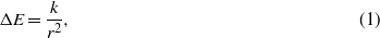
where k is a constant [30]. For example, for the peak at 543 eV, ΔE1 = 10.9 eV, and for the peak at 558.5 eV, ΔE2 = 26.4 eV. It follows that

which agrees well with the ratio of bond length values of SnO2 nanograins, for the second Sn–Sn (=3.19 Å) and first Sn–O (=2.05 Å) coordination shells [31].
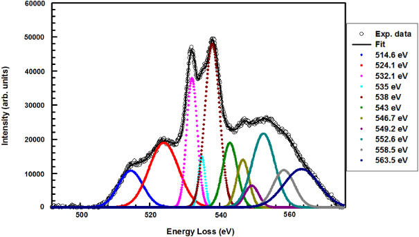
Figure 6. EELS spectrum of the porous SnO2 nanorods with its corresponding fit.
Download figure:
Standard imageWhen incorporating the porous SnO2 nanorods into a sensor platform, by having sawtooth patterned electrodes on the sensor structure, the use of DEP to align the nanostructures becomes more feasible. DEP exploits the dielectric difference between the solvent and the nanostructures in the solvent to induce temporary dipoles that align with the imposed electric field. Because of the geometry of our electrodes, the electric field is greater at the tips of the sawtooth patterned electrodes, which accounts for the preferential alignment of the nanotubes between the tips of opposing sawtooth electrodes [32, 33]. The approach used in this paper also allows for the ability to bury the nanostructure by performing a second electrode deposition on top of the aligned nanostructure, as described previously, allowing improved electrical contact.
The sensor can be tested using the amperometric mode, by applying a voltage between the electrodes and measuring the current between them. Current versus time curves were taken at different operating temperatures (25–500 °C) for sensors using porous SnO2 nanorods as the sensing material. Figure 7 shows the responses to 0.25% CH4 for the different temperatures, where all measurements were taken with an applied voltage of 1.0 V and using air as the baseline gas. The shaded areas on the curves represent the time of CH4 gas exposure. As can be seen, the porous SnO2 nanorod sensor did show a measurable response to 0.25% CH4 at room temperature (figure 7(a)), and it continues to respond all the way up to 500 °C. In addition, as it can be appreciated in figure 7, the baseline at the different temperatures remains reasonably stable throughout the tests.

Figure 7. Porous SnO2 nanorod sensor current versus time curves for 0.25% CH4 in air at 1.0 V. (a) 25 °C, (b) 100 °C, (c) 200 °C, (d) 300 °C, (e) 400 °C and (f) 500 °C.
Download figure:
Standard imageFigure 8 shows the relationship of the sensitivity of the porous SnO2 nanorod sensor to the concentration at various different temperatures. The sensitivity (S) is defined as the ratio of the sensor conductance in the presence of the gas (G) minus the baseline conductance measured in air (G0) to the baseline conductance measured in air (S = (G − G0)/G0). For further clarity, table 1 shows the values of the sensor response to the different concentrations at the different temperatures tested. The values were taken from the plot in figure 8.
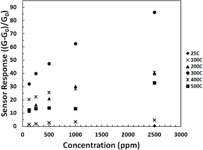
Figure 8. Sensitivity of the porous SnO2 nanorod sensor to different concentrations at the various operating temperatures.
Download figure:
Standard imageTable 1. Sensor response at the various concentrations and temperatures tested.
| Concentration (ppm) | Temperature (°C) | |||||
|---|---|---|---|---|---|---|
| 25 | 100 | 200 | 300 | 400 | 500 | |
| 2500 | 0.58 | 4.8 | 40 | 86.25 | 41 | 30 |
| 1000 | — | 3.6 | 30.3 | 62.5 | 28.3 | 13.5 |
| 500 | — | 2.8 | 21 | 47.5 | 25.7 | 14 |
| 250 | — | 2.2 | 16.3 | 40 | 22.3 | 13.5 |
| 125 | — | 1.6 | 11.7 | 32.13 | 20.3 | 12.5 |
As can be seen from figure 8 and table 1, the optimum operating temperature for CH4 detection at all concentrations tested is 300 °C. At 400 °C, the sensitivity drops to values similar to those at 200 °C. At 500 °C, the sensitivity drops even further and there seems to be little difference in the response between the different concentrations when they are lower than 0.25%. The mechanism for this observed behavior is currently under study, but one possible explanation could be that, at those high temperatures, in metal oxide semiconductors such as SnO2, the mobility of oxygen vacancies becomes appreciable and the mechanism of conduction turns into a mixed ionic–electronic conduction. This is a highly undesirable result that leads to mobile donors and produces slow and irreversible changes in the resistance of the sensor [34]. It is noted that, at room temperature, the only measurable concentration was 0.25% CH4. Below that value, there was no measurable current to be detected. However, the key point to notice is the measurable room temperature sensor response to 0.25% CH4. Figure 9 is a current versus time curve of the sensor at 300 °C for the different concentrations. This is shown to illustrate the typical behavior of the sensor when the methane concentration is lowered.

Figure 9. Current versus time curve for the different concentrations of CH4 tested at 300 °C.
Download figure:
Standard imageFigure 10 illustrates the response time versus temperature plot for each concentration. The response time is defined as the time it takes the sensor conductance to reach a threshold value of ∼90% of the difference between the maximum conductance and the air baseline value. Note that, for each temperature, the response time increases as the concentration is lowered.

Figure 10. Response time versus temperature for each concentration tested. The inset shows the values from 400 °C to 500 °C for more clarity.
Download figure:
Standard imageParallel testing of this sensor structure using solid (non-porous) SnO2 nanobelts without using the carbon nanotube–SnO2 imprinting approach did not show a response to CH4 at room temperature (figure 11). This further confirms our statement that the increase in surface area provided by the unique structure of the porous SnO2 nanorods makes for a more sensitive sensor, in particular at room temperature.

Figure 11. Current versus time curves for 0.25% CH4 in air at 25 °C and 1.0 V for (a) porous SnO2 nanorod sensor and (b) solid, non-porous SnO2 nanobelt sensor.
Download figure:
Standard imageRepeated responses to CH4 were demonstrated. After approximately 190 h of continuous testing, cycling back and forth between the different temperatures, the porous SnO2 nanorod sensor showed an improved response to CH4 at room temperature with little change in the baseline when compared with the previous results, as can be seen in figure 12, thus establishing the sensor's long-term stability.

Figure 12. Porous SnO2 nanorod sensor room temperature response to 0.25% CH4 and 1.0 V after prolonged testing (∼190 h).
Download figure:
Standard imageThe results shown here demonstrate the uniqueness of the porous SnO2 nanorods as a sensing material in that they can detect CH4 from room temperature up to 500 °C. As a result, the porous SnO2 sensor can be used in harsh environments as well. More studies are currently being carried out to test other sensing materials using this same template approach. In addition, floating potential dielectrophoresis (FPD) is being explored as a new alignment method for the porous SnO2 nanorods, as it has been demonstrated to show more control on the alignment of carbon nanotubes [35].
4. Conclusions
In summary, we have fabricated and developed a room temperature methane microsensor using porous SnO2 nanorods as the sensing material. The unique design of the sensor structure combined with the innovative use of the porous SnO2 nanorods makes it the first SnO2-based sensor, to the best of our knowledge, used for room temperature detection of methane without the use of dopants or catalysts. Furthermore, it can be utilized in harsh environments as well, as it also showed sensitivity to higher temperatures (500 °C). Additionally, the sensor was tested at lower concentrations (2500–125 ppm) from 100 °C to 500 °C. At room temperature the lowest concentration that could be achieved was 0.25%. Furthermore, the sensor's stability at room temperature was verified by its improved response after long-term testing (∼190 h). The methane microsensor described in this paper has low power consumption, it is very easy to use and can be applied to a variety of applications, including leak detection of hydrocarbon fuels. It can also be utilized for personal health monitoring and environmental monitoring. The low cost of the simple batch fabrication processes and its compact microsize has the potential for a highly affordable sensor that could be installed in a wide range of locations.
Acknowledgments
The authors would like to acknowledge the contributions of Drs L Matus, M Zeller, and C W Chang for discussions and critical review of the manuscript. We also acknowledge the technical assistance of C Hampton, P Lampard, and M Artale. This research is supported by the Vehicle Systems Safety Technologies Project.