
Abstract
The anisotropy of photoconductivity was measured in InGaAs/GaAs quantum wire heterostructures. This anisotropy is the result of a one-dimensional band creating an effective channel for photo-generated carriers. High photoresponsivity of ∼2.3 A W−1 at 0.3 μW cm−2 incident light excitation was revealed at the InGaAs band edge absorption at room temperature. We show that the observation of this high photoresponsivity at lower power densities is due to the presence of both local electric fields at the InGaAs/GaAs interface caused by structural non-uniformities and a trap at ∼68 meV below the GaAs conductivity band edge. A proposed lateral one-dimensional photoconductive heterosystem is a good candidate for high sensitivity, low-bias infrared detectors.
Export citation and abstract BibTeX RIS
1. Introduction
Recently, semiconductor III–V quantum well (QW) and quantum dot (QD) heterostructures have been intensively investigated for incorporation in infrared photodetectors (IP) based on vertical charge transport [1–4]. In addition, infrared sensors based on lateral charge transport in QDs are possible where the lateral photocurrent is expected to be mainly due to the thermal escape of photo-generated carriers from QDs and thermally assisted electron tunneling into conductive, delocalized states [5–8]. At room temperature, the probability of these processes is high and the lateral photoconductivity (PC) spectra for type-I heterostructures with QDs reproduce the main features of the absorption spectra [9] with some subtle differences due to lateral charge transport.
IPs based on quantum wires (QWRs) have been less thoroughly investigated [10–12] both theoretically and experimentally. The QWR intersubband IPs (QWRIPs) similar to QD intersubband IPs (QDIPs) allow for normal incidence light [3, 10] and have discrete energy spectra allowing flexibility in wavelength engineering of the infrared spectrum, while the dark current of the QWRIP [10] is expected to be smaller compared to the QDIP [9]. In QWR heterosystems, lateral transport is facilitated along the wires. This does not require carrier escape from the QD potential to contribute into PC. This makes QWRs more attractive for the fabrication of lateral transport-based infrared detectors compared to their counterparts based on QDs. In addition, the QWR system can be sensitive to the polarization of incident light [13].
In this paper, we study lateral PC in the InGaAs/GaAs QWR heterosystem for use in lateral transport-based photodetectors for near-infrared applications. These heterostructures contain GaAs Si-doped spacers, which are additional conductive channels of photoexcited carriers that compete with conduction in the main QWR channels. We demonstrate that the QWR heterosystem has enhanced sensitivity to low-intensity normal incident light, which is a result of spatial separation of photoexcited electron–hole pairs by local electric fields produced by non-uniformities in, and potentially around the QWRs.
2. Experimental details
All heterostructures were grown on GaAs (3 1 1)A semi-insulating substrates by molecular beam epitaxy. Following the growth of a 0.5 μm GaAs buffer layer at 580 °C, the substrate temperature was reduced to 520 °C for the deposition of the InGaAs and n-type GaAs barriers. Five periods of InGaAs/GaAs were deposited with 6, 8, 10 and 11 MLs of In0.38Ga0.62As. Each GaAs barrier was 40 nm thick consisting of 10 nm undoped GaAs, then 20 nm uniformly doped GaAs:Si (Nd = 5 × 1017 cm−3), and then another 10 nm undoped GaAs. Finally, each sample was capped with a final InGaAs QWR layer of equal deposition to the buried QWRs for AFM study. Samples with 11 and 10 MLs of InGaAs depositions are shown to form high-quality QWRs [14], while structures with 6 and 8 MLs maintain a QW-like nature. Photoluminescence (PL) spectra were measured at room temperature, using a frequency-doubled Nd:YAG laser at 532 nm for excitation.
For lateral PC studies, mesas aligned along ![$[\bar{2\,}3\,3]$](https://content.cld.iop.org/journals/0268-1242/27/10/105024/revision1/sst438725ieqn1.gif) or
or ![$[0\,1\bar{\,1}]$](https://content.cld.iop.org/journals/0268-1242/27/10/105024/revision1/sst438725ieqn2.gif) crystallographic directions were prepared by wet chemical etching with a photosensitive area 0.75 mm wide. Ohmic contacts separated by 6 mm were formed by annealing indium at 420 °C. PC spectra were measured between 1.0 and 1.6 eV with normal incidence light excitation and a bias voltage of 100 mV. The dark current and the photocurrent were measured over the temperature range of 80–290 K using a current amplifier and standard detection of the direct current.
crystallographic directions were prepared by wet chemical etching with a photosensitive area 0.75 mm wide. Ohmic contacts separated by 6 mm were formed by annealing indium at 420 °C. PC spectra were measured between 1.0 and 1.6 eV with normal incidence light excitation and a bias voltage of 100 mV. The dark current and the photocurrent were measured over the temperature range of 80–290 K using a current amplifier and standard detection of the direct current.
3. Results and discussion
Figure 1(a) presents lateral PC spectra measured along the ![$[\bar{2}\,3\,3]$](https://content.cld.iop.org/journals/0268-1242/27/10/105024/revision1/sst438725ieqn3.gif) direction and PL spectra at 290 K. Low excitation power PL of these structures originates from electronic transitions between confined ground states of the conduction and valence bands of the InGaAs QWRs [14]. The spectral positions of the PL and the turn-on of the PC are in good agreement for each sample. The PC spectra continue to increase beyond this point due to interband electronic transitions in the ensemble of the InGaAs QWRs. The decrease of InGaAs thickness from 11 to 6 ML is detected as a blue shift in PL peak position (see figure 1(a)) and the corresponding PC spectra. For a given temperature, all samples also show a deep valley in the PC for 1.36 < hν < 1.43 eV. The spectral position of this valley is sample independent and is caused by light absorption into defect states in the GaAs as will be shown below. Analysis of both PL and PC spectra will allow us to conclude that for excitation below the GaAs band gap (εg, GaAs = 1.43 eV at 290 K[15]), the measured PC is the result of photoexcited carriers in both the InGaAs and defect states of the GaAs.
direction and PL spectra at 290 K. Low excitation power PL of these structures originates from electronic transitions between confined ground states of the conduction and valence bands of the InGaAs QWRs [14]. The spectral positions of the PL and the turn-on of the PC are in good agreement for each sample. The PC spectra continue to increase beyond this point due to interband electronic transitions in the ensemble of the InGaAs QWRs. The decrease of InGaAs thickness from 11 to 6 ML is detected as a blue shift in PL peak position (see figure 1(a)) and the corresponding PC spectra. For a given temperature, all samples also show a deep valley in the PC for 1.36 < hν < 1.43 eV. The spectral position of this valley is sample independent and is caused by light absorption into defect states in the GaAs as will be shown below. Analysis of both PL and PC spectra will allow us to conclude that for excitation below the GaAs band gap (εg, GaAs = 1.43 eV at 290 K[15]), the measured PC is the result of photoexcited carriers in both the InGaAs and defect states of the GaAs.
In this system, QWRs, the wetting layer (WL), GaAs spacers and interface imperfections can all be channels of conduction for photo-generated carriers. For the doping levels used here, 5 × 1017 cm−3 in the GaAs barriers, these states can be partially populated by the equilibrium electrons and thus have to be considered as potential channels for carrier transport [14, 16]. This is the cause of the large dark conduction, ∼10−4 Ω−1, which was observed in this system.
In order to separate contributions from channels of different dimensionalities, we studied the anisotropy of the PC at different temperatures and levels of light excitation for our structures with different InGaAs thicknesses, and therefore different system dimensionality. The PC anisotropy is defined as ![$\eta = {{I_{[\bar{2}\,3\,3]} }{\big/} { {\vphantom{{I_{[\bar{2}33]} } {I_{[01\bar{1}]} }}}} {I_{[0\,1\,\bar{1}]} }}$](https://content.cld.iop.org/journals/0268-1242/27/10/105024/revision1/sst438725ieqn4.gif) , where
, where ![$I_{[ {\bar{2}\,3\,3} ]}$](https://content.cld.iop.org/journals/0268-1242/27/10/105024/revision1/sst438725ieqn5.gif) and
and ![$I_{[ {0\,1\,\bar{1}} ]}$](https://content.cld.iop.org/journals/0268-1242/27/10/105024/revision1/sst438725ieqn6.gif) are the absolute values of photocurrent that appear for constant applied voltage along the
are the absolute values of photocurrent that appear for constant applied voltage along the ![$[\bar{2}\,3\,3]$](https://content.cld.iop.org/journals/0268-1242/27/10/105024/revision1/sst438725ieqn7.gif) and
and ![$[0\,1\,\bar{1}]$](https://content.cld.iop.org/journals/0268-1242/27/10/105024/revision1/sst438725ieqn8.gif) directions, respectively. This anisotropy was found to be greater than unity for all conditions and all samples, i.e. the photocurrent was found to be higher in the direction along which the QWRs form (see figure 1(b)).
directions, respectively. This anisotropy was found to be greater than unity for all conditions and all samples, i.e. the photocurrent was found to be higher in the direction along which the QWRs form (see figure 1(b)).
For the 8 and 6 ML samples, where QWRs have not formed, the anisotropy changes only slightly with temperature and was found to be about η = 1.5 at both 290 and 80 K (see figure 1(b)). For the samples with QWRs (11 and 10 ML), the anisotropy increases significantly for lower temperature. The temperature dependence of the PC measured along the QWRs for the 11 ML sample is shown in figure 2, with the anisotropy shown in the inset. Here we see an anisotropy increase from 1.5 at 290 K to 3.4 at 80 K. High anisotropy at 80 K for samples with 11 and 10 MLs is an indication of the presence of one-dimensional transport channels for photoexcited carriers due to the QWRs. The anisotropies of the PC as well as the dark conductivity reported in [14] increase as the temperature decreases. This can be understood as the result of the Fermi level dropping with temperature into the lower energy 1D states.
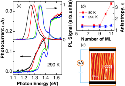
Figure 1. (a) Spectra of lateral PC and PL for InGaAs/GaAs heterostructures with different InGaAs coverages measured at 290 K. The bias voltage of 100 mV was applied along the ![$[\bar{2}\,3\,3]$](https://content.cld.iop.org/journals/0268-1242/27/10/105024/revision1/sst438725ieqn9.gif) direction for PC measurements. (b) Anisotropy of PC as a function of InGaAs thickness measured at 80 and 290 K for hν = 1.36 eV.(c) Schematic diagram of sample biasing used for lateral PC measurements.
direction for PC measurements. (b) Anisotropy of PC as a function of InGaAs thickness measured at 80 and 290 K for hν = 1.36 eV.(c) Schematic diagram of sample biasing used for lateral PC measurements.
Download figure:
Standard image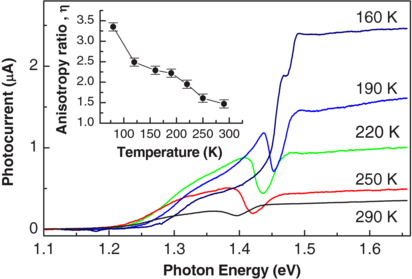
Figure 2. Spectra of lateral PC for 11 ML InGaAs/GaAs QWR heterostructure measured at different temperatures. A bias voltage of 100 mV was applied along the QWRs (![$[\bar{2\,}3\,3]$](https://content.cld.iop.org/journals/0268-1242/27/10/105024/revision1/sst438725ieqn10.gif) direction). The inset represents the anisotropy of PC measured as a function of temperature for hν = 1.36 eV.
direction). The inset represents the anisotropy of PC measured as a function of temperature for hν = 1.36 eV.
Download figure:
Standard imageThe general shape of the PC spectra at different temperatures is independent of the direction of the applied electric field in the plain of QWRs. All spectra show a deep valley at 60–80 meV lower than the band edge of GaAs. This feature exhibits a linear blue shift of ∼5.6 × 10⁻⁴ eV K−1 between 160 and 290 K, which agrees well with the temperature behavior of εg for bulk GaAs. Thus, we suggest that this deep valley in the PC spectra is due to electronic transitions from the valence band of GaAs into the shallow states below the GaAs conduction band edge. These states could be defects close to the InGaAs/GaAs and GaAs/WL interfaces [17]. The formation of free holes due to the above-mentioned transitions will result in their effective recombination with electrons of QWR, WL and GaAs. These recombinations reduce the PC causing the deep minimum in the spectrum. An Arrhenius plot of the photocurrent, ln(IPC) ∼ 1/kT, for hν > 1.5 eV, gives an activation energy of this trap below the GaAs band gap of εa = 67 ± 8 meV. This value agrees well with the position of this PC valley with respect to the GaAs band edge. These states will determine photoresponsivity of the system in the range of the band-to-band transitions of GaAs.
In addition to the transitions between states of the GaAs, the PC spectra show features, which are the result of electronic transitions between ground states of InGaAs (see figure 3(a)). The presence of the InGaAs QWRs appears to introduce a sub-linear dependence of PC versus excitation power density for energies above the QWR ground state (see figure 3(b)). In addition, at higher excitation intensities, there appears a low-energy tail in the PC spectrum for hν < 1.2 eV and T = 290 K. This could be the result of local electrostatic fluctuations of the crystal potential from, for example, local fluctuations of the InGaAs alloy composition, fluctuations of the QWR heights, or interface roughness [18]. Local electrostatic fluctuations within the InGaAs could also be due to ionized donors in the GaAs and ionized defects close to the QWR region. These are all possible mechanisms which will affect charge transport and PC of the InGaAs/GaAs QWR heterosystem.
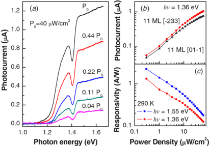
Figure 3. (a) Spectra of lateral PC for 11 ML InGaAs/GaAs QWR heterostructure measured along ![$[\bar{2}\,3\,3]$](https://content.cld.iop.org/journals/0268-1242/27/10/105024/revision1/sst438725ieqn11.gif) direction at 290 K and different levels of light excitation. (b) The photocurrent measured along and across QWRs as a function of excitation power density at light excitation with hν = 1.36 eV and (c) The photoresponsivity measured along the QWRs as a function of excitation power density.
direction at 290 K and different levels of light excitation. (b) The photocurrent measured along and across QWRs as a function of excitation power density at light excitation with hν = 1.36 eV and (c) The photoresponsivity measured along the QWRs as a function of excitation power density.
Download figure:
Standard imageAt low-excitation intensity, for hν > εg, InGaAs, the photo-generated carriers thermalize and fill the lowest energy states, i.e. the minima of the fluctuating InGaAs potential (for example, the QWRs with largest height). Those electrons contribute only slightly to the total PC, because of the local built-in electric fields. At the same time, the non-equilibrium holes are spatially separated from the electrons by the local fields, which decrease electron recombination probability and this results in the enhanced photoresponsivity at 290 K. For increased light intensity, the number of free electrons close to the minima of the potential relief increases, while the defect and impurity states in the GaAs become filled. The excess free electrons and holes will lead to the smoothing of the local potentials allowing for the QWR states and the adjacent GaAs regions to contribute more to the total PC. At the same time, the recombination rate of the non-equilibrium carriers will increase at higher excitation intensities and, thus, the photoresponsivity of the InGaAs/GaAs system decreases (see figure 3(c)). Such behavior is promising for design of low-bias lateral photodetectors with high detectivity, which are sensitive to low-intensity radiation at room temperatures.
4. Conclusions
Studies of lateral PC along the ![$[\bar{2}\,3\,3]$](https://content.cld.iop.org/journals/0268-1242/27/10/105024/revision1/sst438725ieqn12.gif) and
and ![$[0\,1\,\bar{1}]$](https://content.cld.iop.org/journals/0268-1242/27/10/105024/revision1/sst438725ieqn13.gif) crystallographic directions show significant anisotropy that increases for lower temperatures. The degree of PC anisotropy depends on the thickness of deposited InGaAs, which governs the formation of QWRs and, thus, defines conductivity through these states. The appearance of the low-energy 'tail' in the PC spectrum for high-intensity excitation indicates that there are some non-uniformities in, and potentially around, the QWRs, which are responsible for fluctuations of the local potential. The local built-in fields of these non-uniformities separate electron–hole pairs playing a detrimental role in high photoresponsivity of the QWR system at the low-light excitation level at room temperature. Finally, the temperature-dependent PC studies revealed traps with 68 meV below the GaAs conductivity band edge, which sensitize the photoresponsivity of QWR heterosystem as well.
crystallographic directions show significant anisotropy that increases for lower temperatures. The degree of PC anisotropy depends on the thickness of deposited InGaAs, which governs the formation of QWRs and, thus, defines conductivity through these states. The appearance of the low-energy 'tail' in the PC spectrum for high-intensity excitation indicates that there are some non-uniformities in, and potentially around, the QWRs, which are responsible for fluctuations of the local potential. The local built-in fields of these non-uniformities separate electron–hole pairs playing a detrimental role in high photoresponsivity of the QWR system at the low-light excitation level at room temperature. Finally, the temperature-dependent PC studies revealed traps with 68 meV below the GaAs conductivity band edge, which sensitize the photoresponsivity of QWR heterosystem as well.
Acknowledgments
This work was supported by the National Science Foundation through EPSCoR grant no. EPS1003 970.