
Abstract
Studies of the mechanical loss of silicon flexures in a temperature region from 5 to 300 K are presented, where the flexures have been prepared by different fabrication techniques of interest for the construction of suspension elements of future interferometric gravitational wave detectors. A lowest mechanical loss of 3 × 10⁻⁸ was observed for a 130 μm thick flexure at around 10 K. While the mechanical loss follows the thermo-elastic predictions down to 50 K, at lower temperatures the observed loss is found to be a function of surface roughness. This surface loss is of interest for all applications using silicon-based oscillators at low temperatures. The extraction of a surface loss parameter using results from our measurements and those of other authors is presented and the relevance for future gravitational wave detector suspensions is discussed. A surface loss parameter αs = 0.5 pm was obtained. This reveals that the surface loss of silicon is significantly lower than the surface loss of fused silica.
Export citation and abstract BibTeX RIS
1. Introduction
Interferometric gravitational wave (GW) detectors are amongst the most sensitive displacement-measuring instruments ever built. They are designed to search for the effects of tiny fluctuations of spacetime caused by large accelerations of astrophysical objects on the position of mirrors suspended as pendulums. The optical components of a Michelson-like interferometer are suspended as pendulums in order to reduce the effects of seismic noise on the displacement of the optics. The first generation of these detectors like LIGO [1], Virgo [2] or TAMA [3] used metal wires to suspend the test masses. GEO600 [4] pioneered the use of a monolithic suspension system based on fused silica fibres [5, 6] and hydroxide catalysis bonding [7, 8]. Second-generation detectors like Advanced LIGO [9, 10] or Advanced Virgo [11]—which are currently under construction—will adopt this technique [12, 13] amongst others, with the aim of an increase in sensitivity of about an order of magnitude compared to initial detectors. A design study for a third-generation detector of even greater sensitivity has been completed in Europe [14], and in the US, designs are being considered for possible future in situ upgrades to the advanced detectors. In order to achieve any further increase in sensitivity beyond that of second-generation detectors, significant changes in materials and light sources are under consideration (see e.g. [15–19]). Silicon (Si) is a promising candidate material for the test masses and suspension elements for such GW observatories due to its excellent thermal, mechanical and optical properties [20–24]. Silicon is potentially a suitable material for the fabrication of large optical substrates as well as suspension elements in a quasi-monolithic suspension [25–29]. Furthermore, first attempts have been made to demonstrate a full reflective coating based on monolithic grating structures [30–33], thereby removing the requirement for mechanically lossy dielectric optical coatings.
The mechanical loss of a material is a critical parameter in determining the thermal noise performance of an optical component or a suspension (see e.g. [34, 35]). Crystalline materials have in general a larger coefficient of thermal expansion compared to amorphous materials like fused silica. This can result in significant levels of thermo-elastic noise at room temperature [36]; however, the use of crystalline materials like silicon at low temperatures reduces significantly the thermo-elastic noise in the material, as well as potentially reducing the Brownian thermal noise of the material [21, 36, 37].
It has been shown that the mechanical loss of small structures can be expressed as a bulk material intrinsic loss and a surface loss (see e.g. [38–40]). This surface loss can be a significant and limiting source of mechanical loss—especially in small-scale structures like suspension elements or the micro-structured surfaces of optical elements like monolithic gratings. Our investigation focuses on structures whose sizes are relevant for the construction of test mass suspensions and optical micro- and nano-structures. Furthermore, we have exclusively focused on surface preparation techniques that are applicable for elements operating under vacuum for long periods, as will be the case in future GW interferometers.
2. Sample preparation and experimental technique
The silicon flexures were fabricated from high purity float zone grown Si(100) wafers with their long axis parallel to the 〈110〉 direction. All flexures have a thicker block (525 μm) at one end and a thin flexing portion with a thickness between 75–130 μm and a length between 35 and 50 mm (see figure 1(a)).
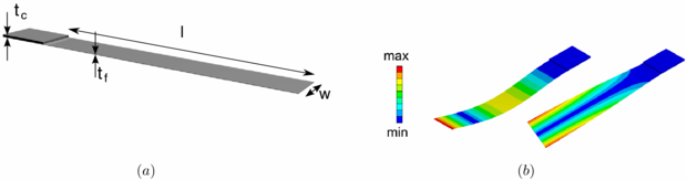
Figure 1. (a) Sketch of the geometry of silicon oscillators used in this study; (b) comparison of the distortion of the bending (left) and torsional (right) modes of the cantilever obtained using finite element analysis. The relative displacement is indicated by the colour in the legend. The second lowest bending mode as well as the lowest torsional mode is shown as examples.
Download figure:
Standard image High-resolution imageThe thin part of the silicon oscillator was obtained using two different techniques [41]: wet chemical etching using a hydroxide solution and dry etching using a reactive plasma. The thick part is used to clamp the samples and to minimize additional energy losses associated with friction in the clamp. Table 1 summarizes the parameters of the samples used in these studies.
Table 1. Summary of the parameters of the Si flexures.
| Properties | Sample 1 | Sample 2 | Sample 3 | Sample 4 |
|---|---|---|---|---|
| Length l (mm) | 35 ± 0.2 | 50 ± 0.2 | 50 ± 0.2 | 50 ± 0.2 |
| Width w (mm) | 4 ± 0.2 | 8 ± 0.3 | 8 ± 0.3 | 8 ± 0.3 |
| Thickness (μm) | ||||
| Flexure tf | 75 ± 2 | 100 ± 5 | 130 ± 10 | 130 ± 5 |
| Block tc | 525 | 525 | 525 | 525 |
| Etching | wet | dry | dry | dry |
| Roughness (rms) | ||||
| Front (etched) (nm) | 33 | 6.8 | 5.9 | 6.2 |
| Back (nm) | 0.9 | 1.9 | 1.6 | 337 |
| (polished) | (polished) | (polished) | (lapped only) |
The samples were intentionally fabricated with different process parameters to obtain different surface finishes (see figure 2). Please note that by tailoring the processes it is possible to achieve higher or lower surface qualities with each individual technique. We chose the different processes in order to span a variety of surface conditions. The wet chemical etching (sample 1) shows etch pits on the surface of the sample. The dry etched samples (samples 2–4) have a smooth surface with small (μm scale) droplets. The rms roughness (measured with a Wyko NT1100 optical surface profiler over a spot size of 600 μm × 450 μm) of the dry etched surface is about a factor of 5 smaller than for the wet chemical etched surfaces. In order to investigate the effect of the surface roughness on the mechanical loss of the sample, a specially treated flexure was produced (sample 4). Here the oscillator was prepared from a single side polished wafer, with the etching process being applied only to the polished side. The result was a silicon flexure with an identical geometry to sample 3 but with one unpolished side—thus having a much higher surface roughness.
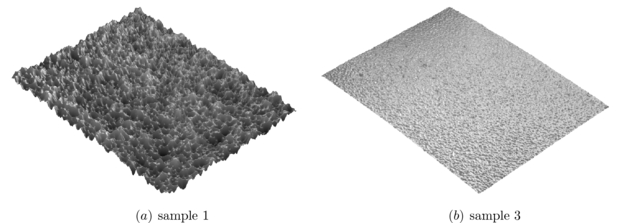
Figure 2. Surface profile of a wet etched (a) and a dry etched (b) sample. Both images were obtained using a Wyko NT1100 optical surface profiler with the same magnification and show an area of 600 μm × 450 μm.
Download figure:
Standard image High-resolution imageThe mechanical loss of silicon flexures was obtained using a mechanical ring-down technique (see e.g. [26, 42]). Here we focused on the bending modes of the sample (see figure 1(b)).
3. Mechanical loss in silicon flexures
The measured loss of a silicon flexure consists of the sum of losses arising from different types of dissipations. These include mechanical dissipation from thermo-elastic losses [43, 44], phonon–phonon scattering losses [44, 45], losses that are related to surface states [39] and impurities [44] or other losses that shall be summarized as excess losses [46].
3.1. Thermo-elastic loss
Zener [43] describes a loss mechanism due to dissipative heat flux in samples under bending oscillation. When a sample flexes, some of its parts are locally heated and some are cooled. These local temperature differences cause heat fluxes that are accompanied by an increase of entropy—or dissipation. In the case of pure bending of a flexure having a rectangular cross-section, the thermo-elastic loss ϕTE is given by [43]

with the coefficient of thermal expansion α, Young's modulus Y, the sample temperature T, the heat capacity per unit mass Cp and the angular frequency ω. τ is a characteristic time given by

where tf is the thickness of the sample and κ the thermal conductivity of the oscillator.
3.2. Phonon–phonon loss
In thermal equilibrium the phonon distribution of a solid is defined by the temperature T. Applying an external oscillation with a typical wavelength much longer than the phonon wavelength (as is the case throughout this paper) results in a modulation of the lattice parameters. This modulation shifts the phonon distribution. The process of redistribution of all phonons to this new local equilibrium forms a loss mechanism referred to as Akhiezer loss, which can be shown to be described by [45]

with the parameter γ = 2.2 as the Grüneisen parameter, v being the speed of sound and τph being the mean phonon lifetime, which can be obtained from the thermal conductivity [45].
3.3. Surface loss
Several authors have pointed out that a mechanical loss contribution of a micro cantilever is dominated by a thin surface layer (see e.g. [38–40, 47, 48]). This layer is thus assumed to have different mechanical parameters compared to the bulk values. The origin of these changes in parameters can be multifold, arising from sources such as local lattice distortions, adsorbed materials on the surface, dangling chemical bonds or surface roughness, and is in general not fully understood [46, 47, 49].
The surface loss contribution, ϕs, for a thin sample under pure bending vibration can be written as (see e.g. [38])

with the surface loss parameter αs = ϕbulkds, where ϕbulk is the intrinsic mechanical loss of the bulk sample. ds represents an effective thickness of the lossy surface layer which is often called dissipation depth, S is the surface area and V the volume of the oscillator. The factor μ is dependent on the mode shape of the oscillation and is given by [38]

with the strain  . A thin flexure under pure bending leads to a value of μ = 3.
3.4. Excess loss
The losses described above are intrinsic to the sample being studied. Additional excess losses can occur through, for example, residual gas damping of the oscillator (see e.g. [46, 50]) or electrostatic losses from the driving plate [46, 51]. These losses can be minimized by a careful experimental design to ensure that they are less than the intrinsic losses studied [26].
3.5. Summary of possible internal loss mechanisms
Figure 3 summarizes the calculated internal mechanical loss contributions, using equation (1) through (4) above, for a typical flexure under investigation in this paper (sample 3 from table 1) for a resonant frequency of 10 kHz. The material properties used were obtained from [52]. For the phonon–phonon loss, we used an experimental value for the thermal conductivity of a sample with a geometry that is comparable with the flexures used in our investigations [53].
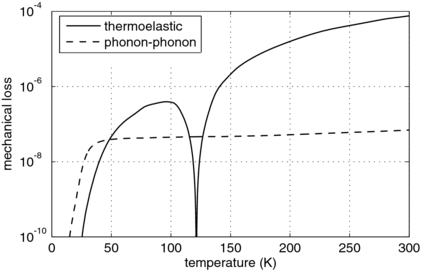
Figure 3. Summary of possible intrinsic loss sources of a silicon flexure at 10 kHz over a wide temperature range. Below 20 K both thermo-elastic and phonon–phonon losses become very small so other loss mechanisms such as surface loss can be studied.
Download figure:
Standard image High-resolution imageThermo-elastic loss dominates at temperatures above approximately 50 K. At around 125 K the effect of thermo-elastic loss is significantly reduced due to the vanishing coefficient of thermal expansion α of silicon at this temperature. At temperatures below about 20 K both the thermo-elastic and phonon–phonon damping mechanisms should decrease significantly for the mode frequencies under investigation, allowing other loss mechanisms such as surface loss to be probed (see section 4.2).
4. Experimental results
4.1. Mechanical loss of silicon flexures at low temperatures
The mechanical losses of several modes of the samples were measured in a temperature range from 5 to 300 K and frequencies between 1 and 70 kHz.
Figure 4 summarizes the results obtained for sample 1. The loss of all modes is limited by thermo-elastic loss at temperatures above 150 K. Below that temperature the modes show an excess loss that is larger than the predicted thermo-elastic limit. The 19.98 kHz mode shows an onset of the thermo-elastic dip at 125 K and reaches a lowest loss of about 5 × 10⁻⁸ at 5 K. All other modes had a lowest loss greater than 10−7. A peak in the loss of the 19.98 kHz mode was observed at a temperature of approximately 20 K. This was not seen for any other mode of this sample; however, the other modes showed higher losses which might have covered the loss peak. Alternatively, this peak could have its origin in a resonant coupling to internal modes of the clamping structure [26].
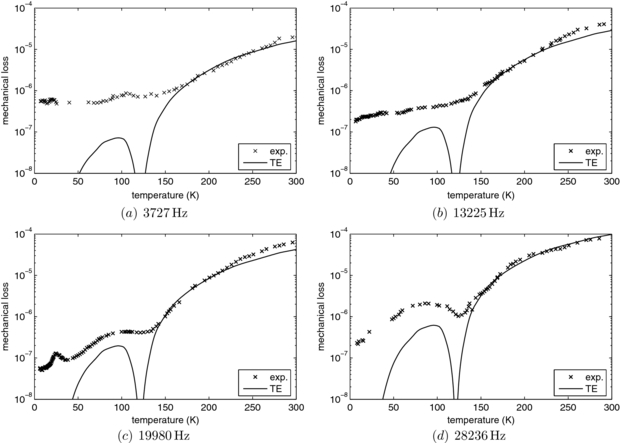
Figure 4. Experimental results of the mechanical loss of sample 1 (wet etched).
Download figure:
Standard image High-resolution imageFigure 5 shows the results for sample 2. In contrast to sample 1 this flexure was fabricated by means of dry etching. The modes follow the thermo-elastic limit down to 150 K. Below that temperature they show evidence of the minima in thermo-elastic damping expected at around 125 K. The third bending mode at 1958 Hz shows an excess loss at temperatures below 125 K, again possibly arising from a coupling between the sample's motion at its resonant frequency and the clamp. The lowest mechanical loss of 4.2 × 10⁻⁸ was observed for the 18.9 kHz mode again at 5 K.
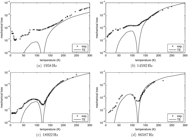
Figure 5. Experimental results of the mechanical loss of sample 2 (dry etched).
Download figure:
Standard image High-resolution imageComparing the results to those of sample 3 (figure 6), it is clear that the excess loss seems to be highest for lower frequency modes. This was a general observation throughout our investigations, here and previously [26]. The results for sample 3 reveal a mechanical loss for this sample reaching values of less than 3 × 10⁻⁸ at around 10 K.
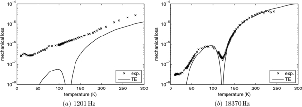
Figure 6. Experimental results of the mechanical loss of sample 3 (dry etching).
Download figure:
Standard image High-resolution imageComparing the lowest losses obtained for each sample at cryogenic temperatures reveals that thin samples have a slightly higher mechanical loss compared to thick samples. This was also seen in other measurements using thin silicon flexures with different thicknesses that are not presented here. This observation is consistent with expectations as thinner samples have a larger surface-to-volume ratio and thus a larger contribution of the surface loss to the overall loss (see equation (4)). In order to confirm the influence of the surface loss, sample 4 was produced with the same geometry as sample 3 but with a rougher back surface (see table 1). The results are summarized in figure 7(a). Both samples show a similar behaviour for temperatures above 50 K. They both follow the thermo-elastic limitation. Below 50 K sample 4 has a lowest mechanical loss greater than 10−7 whereas sample 3 showed a minimum loss of 3 × 10⁻⁸. Both measurements were obtained under similar conditions: 10 K and the 18.4 kHz mode (sixth bending mode), and the results suggest that the surface of the sample, rather than the setup, is limiting the mechanical loss at low temperatures for the samples under investigation.

Figure 7. (a) Investigation of the influence of the surface roughness on the mechanical loss. The sample number corresponds to the sample geometry and treatment given in table 1. Sample 1 is wet chemically etched, sample 3 dry etched with polished backside and sample 4 is dry etched with unpolished backside. (b) Summary of the lowest loss obtained from different sized silicon oscillators. The numbers and letters are explained in table 2 and the text. The plotted line corresponds to a surface loss parameter αs of 0.5 pm. The points A, B and C correspond to bulk sample data where the bulk loss becomes more dominant.
Download figure:
Standard image High-resolution image
Additionally, the measured loss of the wet-etched sample is plotted in figure 7(a). Due to the different geometry of this sample the mode frequencies are not exactly the same. However, a mode close in frequency to the modes used for samples 3 and 4 was chosen to allow comparable conditions. The loss obtained for the wet etched sample is between the losses measured for samples 3 and 4. It would appear that the minimum mechanical loss of the samples is correlated with a decrease in the rms roughness of the surfaces of the samples.
4.2. Analysis of the surface loss
After the influence of the surface on the mechanical loss of the silicon samples at low temperatures was identified, it was possible to extract parameters to characterize the surface loss of silicon. Equation (4) was applied to the available data in order to obtain the surface loss parameter αs. The equation suggests a linear correlation between the mechanical loss and μS/V if the surface loss is the dominating loss source. A wide range of surface-to-volume ratios was used for the investigation (figure 7(b)) taking data from our measurements and from the existing literature. Only those literature values that were measured at sufficiently low temperature (T ⩽ 10 K) where thermo-elastic loss could be neglected have been taken into account. Additionally, only experiments where a stable long-term surface quality was investigated have been included. It is well known that very low surface losses can be obtained for special treatments of the surface, like heating up to 1000 °C for several seconds [48, 54, 55]. However, this lower surface loss is unlikely to be maintained after a short time in cryogenic applications due to surface contamination [55] and thus may be highly difficult to utilize in long duration experiments such as GW interferometric searches. The numbers on the plot indicate the original reference for the values. The key parameters of the different experiments are summarized in table 2.
Table 2. Summary of the parameters of the oscillators from figure 7(b) used to obtain the surface loss parameter from literature values. The mechanical loss ϕ is the measured total loss at the temperature T. The parameter μ is close to the expected values of 3 for bending modes. A larger deviation is observed for modes for bulk samples.
| Point | T (K) | ϕ | μ | Geometry | Reference |
|---|---|---|---|---|---|
| 1 | 4.8 | 1.5 × 10⁻⁴ | 2.98 | 220 μm × 5 μm × 0.06 μm | [56] |
| 2 | 4.2 | 4.0 × 10⁻⁵ | 2.99 | 300 μm × 10 μm × 0.07 μm | [39] |
| 3 | 4.2 | 1.2 × 10⁻⁵ | 2.86 | 260 μm × 3.9 μm × 0.29 μm | [57] |
| 4 | 6 | 5.0 × 10⁻⁶ | 2.94 | 470 μm × 45 μm × 1.5 μm | [58] |
| i | 7 | 5.5 × 10⁻⁸ | 2.96 | Sample 1 | |
| ii | 10 | 5.0 × 10⁻⁸ | 2.96 | Sample 2 | |
| iii | 10 | 3.0 × 10⁻⁸ | 2.97 | Sample 3 | |
| A | 7 | 1.2 × 10⁻⁸ | 2.98 | dia. 100 mm × 0.5 mm | [59] |
| B | 5 | 2.2 × 10⁻⁹ | 2.36 | dia. 6 mm × 12 mm | [60] |
| C | 2 | 5.0 × 10⁻¹⁰ | 0.77 | dia. 106 mm × 229 mm | [61] |
Plotting the mechanical loss at low temperatures (typically below 10 K to allow phonon–phonon as well as thermo-elastic damping to be neglected) of a silicon flexure-based oscillator against its volume-to-surface ratio V/S results in a linear dependence if the mechanical loss is dominated by surface loss (see figure 7(b)). The mode-shape-dependent factor μ was numerically obtained using the FEA package Comsol.
Equation (4) was used to model the data obtained for the thin flexures (1–4, i–iii). It was assumed that the intrinsic bulk loss is much smaller than the surface loss. This is justified by loss measurements on bulk silicon samples that reach values lower than 3 × 10⁻⁹ below 10 K [61]. The only free parameter in equation (4) is the surface loss parameter αs under this assumption. It was adjusted in a way that the resulting linear function corresponds well to the lowest losses of the silicon flexures.
This allows an estimate of the surface loss parameter for silicon samples at temperatures below 10 K of 0.5 pm to be obtained with an accuracy of about 25% which is determined by the error of our own data used for the plot.
The mechanical loss values obtained from the flexures follow the predictions of the surface loss model. The bulk samples show a deviation towards higher losses. Here, the neglected intrinsic bulk loss starts to become significant.
5. Conclusions
We have presented measurements of the mechanical loss of silicon flexures in a temperature range from 5 to 300 K and frequencies from 1 to 86 kHz. At temperatures above 100 K the experimental data follows a trend described by thermo-elastic loss. The observed loss is higher than the thermo-elastic predictions for temperatures below 50 K. The level of the mechanical loss at low temperatures is strongly dependent on the surface quality. Surfaces having a higher rms roughness produce a higher mechanical loss than etched surfaces having a lower rms roughness. The lowest mechanical loss of 3 × 10⁻⁸ was obtained for a 130 μm thick cantilever at a frequency of 18.4 kHz and a temperature of 10 K. Using the lowest mechanical loss obtained from different silicon-based oscillators, it was possible to extract a surface loss parameter following the surface loss model from Gretarsson and Harry of αs = 0.5 pm for temperatures around 10 K. This value is at least an order of magnitude smaller than that for fused silica [62]. Together with its remarkable mechanical and thermal properties, the low surface loss makes silicon a very promising material for low mechanical loss applications at cryogenic temperatures, such as the suspension elements in future GW detectors. However, the microscopic origin of the surface loss as well as its temperature and frequency dependence are still not fully understood and will be the subject of further investigations.
Acknowledgments
This work was in part supported by the German Science Foundation under contract SFB TR7 and the STFC in the UK. RN was supported by the FP7 EU project Einstein Telescope Design Study under contract number 211743. IWM holds a Royal Society University Research Fellowship. SR holds a Royal Society of Edinburgh Research Fellowship and SR is a Royal Society-Wolfson Research Merit Award holder. The authors would also like to thank the University of Glasgow, and the Scottish Founding Council for support for this work. We also wish to thank B Höfer from the Fraunhofer Institute für Angewandte Optik und Feinmechanik for support in the sample preparation. We would like to thank P Hanse and S Eiweleit for their support constructing the setup. The help of L Föllmer and T Eismann is kindly acknowledged during the cryogenic runs. We would like to thank our colleagues in the GEO600 and LIGO Scientific Collaborations for their interest in this work.