
Abstract
We have attempted to establish a unified theory of SiC oxidation by reproducing all the SiC oxide growth rates on the (0 0 0 1) Si-face, (1 1  0) a-face and (0 0 0
  ) C-face at various oxidation temperatures and oxide partial pressures. Growth rates were calculated using the Si and C emission model and were confirmed to fully reproduce the observed data when an enhanced surface oxide growth rate was added to the previously defined growth rate. The parameters deduced from the calculations indicated that the activation energy for the initial interfacial reaction rate corresponds to the number of Si back-bond(s) on the crystalline surface. Although the C emission ratio was found to have no significant dependence on the surface orientation, the Si emission ratio varied significantly and so likely determines the oxide growth rate. The densities of Si and C interstitials at the SiC-oxide interface were simulated both on the oxide and SiC substrate sides, and the optimal oxidation sequence is discussed in terms of the formation of the interface state.
Export citation and abstract BibTeX RIS

Original content from this work may be used under the terms of the Creative Commons Attribution 3.0 licence. Any further distribution of this work must maintain attribution to the author(s) and the title of the work, journal citation and DOI.
1. Introduction
Silicon carbide (SiC) is an attractive material for power device applications owing to its superior properties, including a wide bandgap, a high breakdown field and high thermal conductivity, allowing the design of extremely low power loss devices [1]. In addition, SiC is highly resistant to radiation, and thus is well suited for applications in nuclear plants or spacecraft [2]. Furthermore, SiO2 films can be grown on SiC substrate surfaces by ordinary thermal oxidation [3]. However, with regard to the development of various SiC devices, the optimization of the SiC oxidation sequence is often crucial to achieving the potential device performance.
It is important to obtain a deeper understanding of the SiC oxidation mechanism because it is closely related to the performance of high-voltage bipolar devices [4] as well as metal oxide semiconductor field effect transistors (MOSFETs) [5]. For example, the oxidation of a SiC substrate is a promising means of eliminating deep-level states, so-called Z1/2 centers, that act as lifetime killers in the drift layer [6]. With regard to the development of MOSFETs, improving the quality of the oxide-SiC interface is the key to obtaining low power loss [1], and clarification of the oxidation mechanism should be of significant assistance in this regard [5].
Approximately fifty years ago, a linear-parabolic oxide growth equation, the so-called Deal-Grove (DG) model, was proposed as a theoretical model for Si oxidation [7]. Although this equation describes the typical oxide growth rate on Si, it does not reproduce the growth rate within a few tens of nanometers, regardless of parameter tuning. Twenty years later, Massoud et al proposed an empirical equation based on the DG equation together with an additional exponential term that represents the growth rates within a few tens of nanometers [8]. This new equation successfully reproduced the oxide growth rates over the entire thickness region. However, the exponential term was not based on physical considerations. More recently, Kageshima et al established a theory that describes the complete oxide growth process, including the oxide growth rate within a few tens of nanometers [9]. According to this model, Si atoms are emitted as interstitials into the oxide layer, accompanied by the oxidation of Si, which is caused by the strain due to expansion of the Si lattice during oxidation. The oxidation rate at the interface is initially high but is later suppressed by the accumulation of emitted Si atoms near the interface with increasing oxide thickness.
It has been reported that the DG equation is also applicable as a SiC oxide growth equation for the description of experimentally obtained oxide growth curves [3, 10–12] when certain coefficients that take into account the oxidation of C are included with the oxidation rate parameters [11]. Despite this, both real-time and conventional measurements of oxide growth rates have revealed that there is a high growth rate region during the formation of a layer a few tens of nanometers in thickness that cannot be described by the DG equation, and that the Massoud empirical equation better reproduces SiC growth rate data, similar to the case of Si oxidation [13–18]. Based on these results, we have proposed a SiC oxidation model, termed the Si and C emission model, that takes into account both Si and C emission into the oxide, both of which reduce the interfacial reaction rate [5, 19]. The calculated oxide growth rates based on this model agree with experimental growth rate data, including those within a thickness of a few tens of nanometers. In addition, we have succeeded in the direct observation of Si emission into the oxide layer via depth profiling of an oxidized HfO2/SiC structure [20]. Our group has also investigated the effects of Si and C emission on the oxidation rate by real-time measurements of the oxide growth rate. Experimental observations of annealing-inserted oxidation and two-temperature oxidation indicated that this emission suppresses the oxidation rate [20], demonstrating the validity of the Si and C emission model. However, the observed growth rate data were restricted to the (0 0 0 1) Si-face and  C-face; therefore, it has been difficult to discuss the overall oxidation mechanism of SiC. Very recently, oxide growth rate data for the
  -face as well as the Si-face and C-face were obtained using in situ spectroscopic ellipsometry [17].
Although the origin of the SiC MOS interface state has not yet been completely clarified, there have been several reports that identified the Si/C interstitials emitted into the oxide/SiC substrate as a trigger for the formation of interface states. For example, Hashimoto et al reported that there is a strong correspondence between the interface state density and the refractive index of the interface layer determined by spectroscopic ellipsometry measurements, which is affected by the density of Si interstitials in the surface layer of the SiC substrate [21]. Also, Afanasev et al [22] suggested that a graphite-like carbon layer forms near/at the interface, which causes interface states over the entire range of the forbidden energy band. In addition, intrinsic SiO2 defects (near interface traps; NITs), which presumably originate from oxygen deficiency, are present regardless of the Si or SiC polytypes, and give rise to interface states in the vicinity of the 4H-SiC conduction band edge. Oxygen deficiency can be regarded as the presence of Si interstitials in SiO2; therefore, Si (Si and C) emission into the SiO2 layer may be the origin of these SiO2 defects. According to ab initio studies performed by Knaup et al, NITs originate from Si interstitials or C dimers that in turn are produced by C interstitials inside the SiO2 [23, 24]. However, according to ab initio studies by Devynck et al [25, 26], the C–C pairs in SiC that originate from C interstitials and the Si–C–O structure give rise to a broad peak in the interface state density, while the Si2–C–O structure produces a sharp peak near the conduction band edge, which is compatible with an NIT. Cochrane et al employed an electrically detected magnetic resonance (EDMR) technique and identified Si vacancies (or C dangling bonds) in the SiC side near the interface [27], which can presumably be attributed to Si emission during oxidation. Recently, Shen and Pantelides identified the origin of interface states that degrade the SiC MOS channel mobility as C di-interstitials that are formed by a combination of two C interstitials injected into the SiC substrate [28]. It is thus considered that analysis of the interfacial Si and C interstitials emitted during oxidation should provide the key to realizing an ideal MOS interface.
In this report, a unified theory that accounts for all the observed growth rates is established using the oxide growth rate data for the Si-face, C-face and  -face at various oxidation temperatures and oxide partial pressures. The mechanism for the oxidation of SiC is discussed in terms of the oxidation rate parameters deduced from calculations. Simulations of Si and C interstitial density variations were also conducted to optimize the oxidation sequence with respect to a reduction of the interface state density.
2. Model for oxide growth rate calculation
Figure 1 shows schematic diagrams of the oxide growth rate for SiC over the entire oxide thickness region. The oxidation processes are categorized into four stages: (i) surface oxidation stage, (ii) interface oxidation stage, deceleration region, (iii) interface oxidation stage, steady-state, and (iv) diffusion-limited stage. In the DG model [7] and the Massoud empirical relation [8], it is assumed that oxide growth occurs only or mainly at the Si-oxide interface (so-called passive oxidation [29]), which corresponds to stages (ii) and (iii). However, in the interfacial Si emission model [9], Si atoms are emitted into the oxide layer, some of which encounter the oxidant inside the SiO2 layer to form SiO2. While the number of emitted Si interstitials increases with the oxide thickness, the interfacial reaction rate, i.e. the oxide growth rate, is suppressed because the accumulation of Si interstitials prevents the oxidation reaction around the interface, as in stage (ii). In the case of SiC oxidation, both C and Si emission occurs and suppresses the interfacial reaction rate during oxidation. The diffusivity of C interstitials is much higher than that of Si interstitials; therefore, the accumulation of C interstitials becomes saturated prior to that of Si interstitials [19]. Following stage (ii), the concentration of Si interstitials becomes saturated and the oxide growth rate becomes constant when the accumulation and consumption of Si interstitials is balanced [17] (stage (iii)). In the DG model, only such an unchanged interface oxide growth rate, i.e. a linear oxidation rate B/A, is taken into account for the interface reaction rate-limiting region [7]. In addition to these stages, when the oxide is very thin, some of the emitted Si atoms can pass through the oxide layer and reach the oxide surface, where they are instantly oxidized, which results in the formation of a SiO2 layer on the oxide surface (active oxidation [29]), as in stage (i). In stage (iv), the diffusion of oxidants in the oxide is the rate-limiting process, as traditionally described by the DG model [7]. Note that the growth rate in stage (iv) should be weakly dependent on the surface orientation because it is determined by the diffusion of the oxidant in SiO2, which is independent of the interface oxidation reaction. Next, we consider the dependence of the oxide thickness on the Si and C concentrations at the interface. In stage (i), the concentrations are very low because most of the interstitials reach the oxide surface and are instantly oxidized at the oxide surface or are otherwise evaporated into the gas phase. In stage (ii), these interstitials increase with oxide thickness. After the accumulation of interstitials becomes saturated (stage (iii)), emission to the SiC substrate side begins to increase [30, 31]. In stage (iv), oxidant diffusion limits the growth rate, so that the oxide growth rate (or interstitial emission rate) is reduced, and the concentrations of Si and C interstitials in the oxide side decrease [32], while those in the substrate side increase slightly [33].
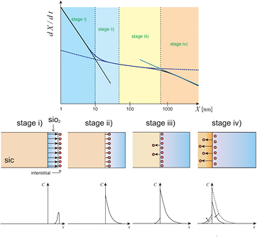
Figure 1. Schematic diagrams of the oxide growth rate for SiC over the entire oxide thickness region.
Download figure:
Standard image High-resolution imageAccording to the interfacial Si emission model [9], the interfacial reaction rate k, is a function of the oxide thickness and the oxidation rate is not enhanced in the thin oxide region, but is quickly suppressed with increasing thickness. To describe this change in k, Kageshima et al introduced the following equation [9, 32]:
where k0 is the initial interfacial oxidation rate, and  and C0 are the concentrations of interstitials at the oxidizing interface and the solubility limit, respectively, where the subscript denotes the corresponding atom. It should be noted that k is constant in the DG model. The total growth rate, including the surface, internal and interface oxidations, is given by the sum of these three oxidation processes, as [9]:

where ν is the emission ratio, κ is the oxidation rate of Si interstitials inside SiO2, η is the oxidation rate of Si interstitials on the oxide surface, N0 is the molecular density of SiO2 ( cm−3), and the superscript 'S' denotes the position at the oxide surface (x = X). The first, second and third terms on the right-hand side of equation (2) correspond to the interface oxide growth, the oxide growth inside SiO2 and the surface oxide growth, respectively. The concentrations of Si interstitials and O2 molecules in SiO2 (
 and
and  , respectively) are derived using a numerical calculation based on diffusion theory [32]. The associated diffusion equations are provided in the next section. If a steady-state approximation is assumed during the calculations, then the obtained growth rate equation is equivalent to the Massoud empirical relation [9].
In the case of SiC oxidation, both C emission and Si emission should be taken into account because SiC consists of Si and C atoms. Although the oxidation was carried out through the heating of a 6H-SiC/glass structure, Hähnel et al suggested that there are four oxidation stages in SiC oxidation that have different oxidation reactions, including Si and C emission processes [34]. On the other hand, according to the thermodynamic model proposed by Song and Smith [35], the oxidation reactions on the SiC surface can be summarized as follows.

where reactions (a) and (c) represent oxidation associated with C and Si emission, respectively, and reactions (b) and (b') represent passive oxidation. A lower temperature or higher partial pressure will result in reaction (a) becoming dominant, while a higher temperature or lower pressure will promote reaction (c). According to recent results reported by Goto et al, the extent of CO2 production is negligible [17], regardless of the surface orientation or oxidation temperature. Therefore, reaction (b') in equation (3) can be excluded. Although the frequency of each process depends on the temperature and partial pressure, it is believed that reactions (a)–(c) occur simultaneously during oxidation [20]. Hence, the following relationship can be written in accordance with principle of mass conservation:

In the case of Si oxidation, the interfacial reaction rate (equation (1)) can be introduced by assuming that  does not exceed
  , although the reaction rate decreases with increases in
  . Based on this concept, the interfacial reaction rate for SiC can be derived by multiplying decreasing functions for Si and C [19]:

Evidence for the validity of equation (5) is provided in [20].
Diffusion equations for Si and C interstitials and for oxidants can be written by modification of those generated by the interfacial Si emission model [32]:

where the prime indicates the value for C atoms and h is the gas phase mass-transfer coefficient [7]. It is worth noting that R2 and  represent the absorption of interstitials inside the oxide and are each assumed to consist of two terms, as suggested by Uematsu et al [36]. From equation (4), the boundary conditions at the interface are given by:
It has been stated that the oxidation rate in the thick oxide region is limited solely by the in-diffusion of the oxidant [17, 18], and that the diffusivity of CO in SiO2 is much faster than that of O2 [19]. Thus, it was assumed that the diffusion of CO is independent of the oxide growth rate. The oxide growth rate is described by equation (2); however, the second term on the right-hand side (i.e. the absorption of Si interstitials inside the oxide) is modified to the combination of  and
and  given in equation (6) (see equation (6) in [19]). This integral term was approximated as described in [19]. Equations (5–7) were solved numerically using the partial differential equation solver ZOMBIE [37]. The oxide thickness X, at each time step was obtained from equation (2). The parameters related to the properties of SiO2 (
 ,
,  , η,
, η,  ,
,  and
and  ) were taken as equal to those obtained from Si oxidation studies [32, 38]. The parameters regarding C interstitials (
 and
and  ), and the values of k0 and
  were determined by fitting the calculated oxide growth rates to the measured oxide growth rates.
3. Experimental
4 H-SiC (0 0 0 1) Si-face (n type,  cm−3,
cm−3,  off), 6 H-SiC
  -face (n type) and 4 H-SiC
  C-face (n type,
  cm−3,
cm−3,  off) substrates were used as samples. Note that the differences induced in the growth rates due to the polytype [10] or off-angle were within the measurement errors. Oxidation was conducted using an infrared lamp heater at temperatures between 900 and 1200 °C under an oxygen flow of 1000 sccm and oxygen partial pressures from 0.02 to 1.0 atm. Prior to oxidation, the optical constant of the SiC at the oxidation temperature was measured under an Ar atmosphere. The Ar was then replaced with oxygen and real-time measurements of ellipsometric parameters
  were performed. The wavelength range of 310–410 nm was selected for oxide thickness analysis to avoid radiation or light reflection from the samples. The angle of incidence was 75.8°. When determining the oxide thicknesses from
  spectra, a three-layer structure was assumed as the analysis model, which consisted of SiO2/interface layer/SiC. Details of the analysis method have been described elsewhere [16, 39].
4. Results
4.1. Oxygen partial pressure dependence
Figure 2 shows the dependence of the oxide thickness on the oxide growth rate for (a) the Si-face and (b) the C-face at various oxygen partial pressures and 1100 °C. The dashed curves denote growth rates calculated using the Si and C emission model. Only  depended on the partial pressure as
  (1 atm), while all the other parameters were constant at all partial pressures. Although the calculated curves are in agreement with the experimental data above 10 nm, they differ below 10 nm, and the discrepancy becomes larger as the pressure is lowered. Considering the calculated curve, the initial rate deceleration becomes insignificant with decreasing pressure, which is the opposite of the trend in the experimental data. This contradiction has also been noted in the case of the oxide growth of Si [40] and is likely due to an underestimation of the surface oxide growth rate [41].
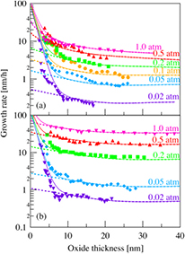
Figure 2. Dependence of the oxide thickness on the growth rates for the (a) Si-face and (b) C-face at various oxygen partial pressures and 1100 °C. The solid and dashed curves represent growth rates calculated using the Si and C emission model with and without enhanced surface oxide growth rate, respectively.
Download figure:
Standard image High-resolution image4.2. Surface orientation dependence
Figure 3 shows the dependence of the oxide thickness on the oxide growth rates for (a) the Si-face, (b) the a-face and (c) the C-face at various oxidation temperatures and 1.0 atm. The dashed curves represent the growth rates calculated using the Si and C emission model. Taking the discrepancy in the surface oxide growth rate into account, the calculated curves correspond to the experimentally observed growth rates above a few tens of nanometers. Similar to the partial pressure dependence, the growth rates within a few tens of nanometers tend to deviate from the calculated growth rates, especially for the Si-face.
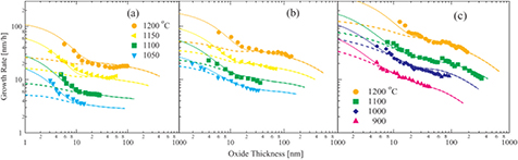
Figure 3. Dependence of the oxide thickness on the oxide growth rates for the (a) Si-face, (b) a-face and (c) C-face at various oxidation temperatures and 1.0 atm. The solid and dashed curves represent the growth rates calculated using the Si and C emission model with and without enhanced surface oxide growth rate, respectively.
Download figure:
Standard image High-resolution imageFigure 4 shows Arrhenius plots of the initial interfacial oxidation rates k0 and emission ratios ν as determined from the curve fits. The activation energies of k0 for the Si-, a- and C-faces were found to be 0.68, 1.37 and 2.02, respectively. It should be noted that the ratio of the activation energies for these surface orientations is consistent with the number of Si back-bond(s) at the oxidation interface [42]; one Si–C back-bond for the C-face, two for the a-face and three for the Si-face [17]. Thus, k0 indicates the surface oxidation reaction rate for the substrate, which is dependent on the surface structure. If we consider that oxidation consumes energy proportional to the number of Si–C bonds to be broken, then it is reasonable that the ratio of the activation energies of k0 corresponds to the number of Si back-bonds. Therefore, it is confirmed that k0 is self-consistent when using the definition in the Si and C emission model. In figure 4(b), the C emission ratios  are almost equal for each surface orientation. In contrast, the Si emission ratios
  are dependent on the surface orientation; those for the Si-face and the a-face are the largest and the second largest, respectively. Figure 3 shows that the oxide growth rates during stages (ii) and (iii) (the interface oxidation stage) for the Si-face and the a-face are the lowest and the second lowest, respectively. Therefore, the oxide growth rate during these stages is predominantly determined by
  and k0.
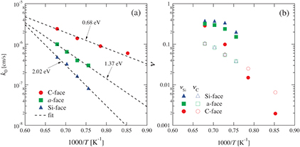
Figure 4. Calculation parameters deduced from curve fits: (a) initial interfacial oxidation rate k0 and (b) emission ratio, ν.
Download figure:
Standard image High-resolution image5. Discussion
5.1. Enhanced surface oxide growth
We first consider the difference between the calculated and observed growth rates in the region extending to 10 or 20 nm. It was experimentally confirmed [20] that in the very early stage of oxide growth, surface oxide growth is the main growth process. In addition, the growth mode transitions to interface oxide growth after oxide growth of approximately 1.2 nm at 1100 °C. Kouda et al also suggested that the rapid deceleration in the very early growth stage is explained by the dependence of the oxide thickness on the surface oxidation rate because the growth rate is not significantly different between the Si- and C-faces [16]. In addition, the dependence of the oxide thickness on the surface oxidation rate is represented by an exponential attenuation function [16]. We have specified that the surface oxide growth is enhanced to a greater extent than is assumed in the Si and C emission model, and the calculated growth rate is almost consistent with the observed growth rate assuming a 104 times higher density of oxygen (i.e.,  ), which approximately corresponds to the ambient gas phase oxygen [5, 43]. However, such a high oxygen density causes a discontinuity in the Si interstitial distribution; therefore, the calculation readily fluctuated and returned erroneous results. Accordingly, an exponential term was included to account for the enhanced surface oxide growth rate, as previously discussed by Kouda et al [16]:

where  and
and  are the maximum surface growth rate and the characteristic length at which active oxidation transitions to passive oxidation, respectively. The solid lines in figure 2 are the curves calculated with the addition of equation (8), where
  and 130 nm h−1 for the Si- and C-faces, respectively, and
  nm for both faces at any pressure. The calculated growth rate curves successfully reproduce the observed curves, including the surface oxide growth region.
The growth rates with this enhanced surface oxide growth rate were also calculated at various temperatures for the three surface orientations, as shown in figure 3 (solid lines), where a common value of  between the surface orientations was applied for each temperature. The modified growth rate curves exactly reproduce all the experimentally observed growth rates, which strongly supports the validity of this modification. Figure 5 shows Arrhenius plots of the surface oxidation parameters,
  and
and  . The activation energies of
  were obtained by fitting to be 2.02 and 1.01 eV for the Si- and C-faces, respectively. The activation energy of
  for the Si-face agrees with that of k0. Therefore, in the case of the Si-face, the surface oxide growth rate is predominantly determined by the initial interfacial reaction rate. In contrast, the activation energy of
  for the C-face does not agree with that of k0, but rather with that of
  (1.07 eV [32]). According to the report from Kageshima et al [9, 44], in the case of SiO2 growth on Si, the maximum surface growth rate K that corresponds to
  is proportional to
  , which fully supports the present results. Therefore, the factor that determines
  for the C-face is considered to be the surface oxidation rate, which is similar to Si oxidation. For the a-face, the value of
  appears to be outside of the Arrhenius relation, and this can be interpreted as showing that the rate-limiting factor is intermediate between the interface and surface reactions. In figure 5, the value of
  decreases with decreasing temperature and eventually levels off, and the values are in approximate agreement with L for the Si-face in reference [17]. Initial surface oxidation is more significant for the Si-face; therefore, it is considered that the value of L for the Si-face corresponds to
  .
.
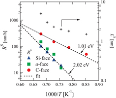
Figure 5. Calculation parameters deduced from curve fits: (a) the maximum surface growth rate  and (b) the characteristic length,
  .
.
Download figure:
Standard image High-resolution image5.2. Interface oxide growth deceleration
In stages (ii) and (iii), the oxide growth predominantly occurs at the oxidation interface, and the interfacial reaction rate (k) is suppressed due to the accumulation of Si and C interstitials, as given by equation (5) [20]. Goto et al recently reported that the ratio of steady oxide growth rate (B/A) and initial oxide growth rate (B/A + C) is approximately 1/5, irrespective of the oxidation temperature and surface orientation [17]. The values of C and B/A correspond to  and
and  in the Si and C emission model, respectively, where
  is the minimum value of k when the Si and C interstitials exhibit the greatest extent of accumulation. Here, we define the function f as
  to take into account that
  in this thickness region (i.e.
  ). Figure 6 exhibits the f curves as a function of the oxide thickness obtained from calculations at temperatures of 1100 and 1200 °C for the three surface orientations. The f values increase to almost the same maximum (4–6) at a thickness between 10–100 nm, regardless of the temperature and surface orientation, which is consistent with the results reported by Goto et al [17]. Therefore, the degree of deceleration between stages (i) and (iii) is not significantly dependent on the temperature or the surface orientation.
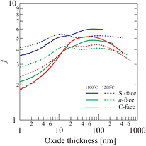
Figure 6. Calculated f curves as functions of oxide thickness at temperatures of 1100 and 1200 °C for the three surface orientations.
Download figure:
Standard image High-resolution image5.3. Simulations of interface interstitial concentration
The Si, C and O interstitial concentrations at the interface on the oxide side ( ) were obtained from the growth rate calculations. Note that these concentrations were estimated from the interface oxide growth process; therefore, the interstitials that contribute to the surface oxide growth were ignored. However, these are still valid because the interstitials for surface oxide growth do not accumulate near the interface, as noted in section 2. Despite this, additional calculations must be conducted to determine the Si and C interstitial concentrations at the interface on the SiC substrate side (hereafter denoted as
  ).
).
According to Kawahara et al [45], the C interstitial distribution  , can be calculated using diffusion theory:

where  and γ are the concentration of C vacancies and the recombination coefficient between an interstitial and a vacancy, respectively. Accurate oxide growth rates were determined for the boundary conditions, although Kawahara et al approximated these by assuming the values to be proportional to the inverse αth order of the oxidation time (
 or 0.48) [45]. Therefore, the boundary and initial conditions are expressed as:

where  and
and  are the emission ratio on the substrate side and the molecular density of 4 H-SiC (
 [46]), respectively. According to Kawahara et al [45], the activation energy for C interstitial flux at the interface (F0) is 1.4 eV, which is almost equal to that of
  . Therefore,
  can be estimated from the relationship
  . The value of a is calculated to be
  from that of F0. The initial concentration of C vacancies
  , is set to 1013 cm−3, which is typical for 4H-SiC epiwafer [45].
For calculations of Si interstitials, the following diffusion equation is used [43]:

with boundary and initial conditions as follows:

where the Si emission ratio is obtained from the relationship  , which is similar to the case of C interstitials. The values of
  are obtained from the relationship
  [cm2 s−1], where
  and T are the Boltzmann constant and the absolute temperature, respectively. The activation energy was obtained from the literature [47] and the exponential term was determined by comparison between the thicknesses at which
  increases and
  is saturated because these thicknesses must be the same as described in section 2.
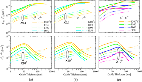
The solid curves in figure 7 represent the oxide thickness dependence of  and
and  for the Si-, a- and C-faces at various oxidation temperatures and an oxygen pressure of 1.0 atm. During stages (i) and (ii),
  increases with X and becomes saturated because of Si emission and Si absorption due to oxidation balances. However, after the beginning of stage (iv),
  is reduced because
  is lowered by the reduction of
  , as discussed by Uematsu et al [38]. However,
  increases until a few tens of nanometers and then decreases. Therefore, since C-related defects in the oxide are thought to give rise to interface states over the entire forbidden band [22, 25, 26], oxide growth up to a few tens of nanometers should be avoided at the point at which
  becomes a maximum. This variation is explained by the accumulation of C interstitials prior to Si interstitials because the diffusivity of the C interstitials is greater [19]. After the accumulation of C interstitials becomes saturated, that of Si interstitials still continues, which leads to a reduction of
  and to a decrease in
  .
.
Figure 7. Dependence of the oxide thickness on the Si and C interstitial concentrations at the interface with the (a) Si-face, (b) a-face and (c) C-face at various oxidation temperatures and 1.0 atm. The solid and dashed curves represent the concentrations on the oxide side ( ) and substrate side (
 ), respectively.
Download figure:
Standard image High-resolution image
The dashed lines in figure 7 show the dependence of the oxide thickness on  and
and  for the Si-, a- and C-faces at various oxidation temperatures and an oxygen pressure of 1.0 atm. For the Si- and a-faces, a higher temperature corresponds to a lower value of
  . In contrast, for the C-face, a higher temperature corresponds to a greater value of
  , although the values at 1100 and 1200 °C are comparable. In addition, for the Si- and a-faces, the value of
  levels off at around several nanometers and then increases again from a few tens of nanometers. As Taniguchi et al [30] reported for Si oxidation, the Si emission rate into the substrate is enhanced when
  becomes saturated (see stage (iii)) in figure 1). In contrast, this plateau of
  is rarely observed in the case of the C-face. This is explained by considering that the diffusion-limiting step (stage (iv)) starts just after the accumulation of
  ends, which is similar to the situation for Si oxidation [38]. With regard to the variation of
  , the increase in the oxide thickness dependence is almost monotonic. In addition, elevated temperatures result in higher values of
  for all the surface orientations. Therefore, a thinner oxide and a lower oxidation temperature should be selected to obtain fewer C interstitials in the SiC substrate.
6. Conclusion
An attempt was made to reproduce the oxide growth rates of SiC for various oxidation temperatures, oxygen partial pressures and surface orientations of the substrate based on the Si and C emission model. All the oxide growth rates were successfully reproduced using the model and taking into account enhanced surface oxide growth. The difference in the oxidation processes due to the different surface orientations was discussed in terms of parameters deduced from the calculations. The activation energies for the initial interfacial reaction rates between these surface orientations were consistent with the quantity of Si back-bonds, indicating that the proposed model is valid, because the energy necessary for oxidation should be proportional to the number of Si back-bonds to be broken. Furthermore, the growth rate for the interface reaction-limiting step was determined not by the C emission ratio, but by the Si emission ratio, just as for the initial interfacial reaction rate. The maximum surface growth rate was dependent on the surface orientation, likely due to the difference in the rate-limiting step for this oxidation stage. In contrast, the characteristic length at which the surface oxidation transitions to interface oxidation was common between these surface orientations. This is also explained by considering that the characteristic length is determined by material properties of SiO2 such as the diffusivity of Si interstitials. The deceleration in the degree of interface oxide growth was almost constant, irrespective of the oxidation temperature or surface orientation, which was confirmed by calculations of the deceleration function.
The interface Si and C interstitial concentrations were simulated using the proposed unified SiC thermal oxidation model. The simulations indicated that the concentration of Si interstitials at the oxide side becomes saturated around an oxide thickness of several tens of nanometers, while that at the substrate side increases again. The concentration of Si interstitials then begins to decrease in the diffusion-limiting step. The concentration of C interstitials at the oxide side has a maximum at a thickness of a few tens of nanometers, while at the substrate side the concentration increases monotonically with the thickness. The effect of the oxidation temperature on the concentrations of C interstitials at both the oxide and substrate sides increased with increasing temperature.
In conclusion, a unified theory that describes all the oxidation stages of SiC under various oxidation conditions (that is, various temperatures and oxygen partial pressures) and with different surface orientations of the substrate could be established based on the Si and C emission model. We have demonstrated that this theory enables the design of an optimum oxidation sequence and prediction of the interface structure.
Acknowledgments
The authors thank Dr Nishino of the Kyoto Institute of Technology for providing a (11–20) a-face substrate. This work was supported in part by Grants-in-Aid for Scientific Research from the Japan Society for the Promotion of Science (#15H03967).