

Abstract
The probing and modeling of carrier motions in materials as well as in electronic devices is a fundamental research subject in science and electronics. According to the Maxwell electromagnetic field theory, carriers are a source of electric field. Therefore, by probing the dielectric polarization caused by the electric field arising from moving carriers and dipoles, we can find a way to visualize the carrier motions in materials and in devices. The techniques used here are an electrical Maxwell-displacement current (MDC) measurement and a novel optical method based on the electric field induced optical second harmonic generation (EFISHG) measurement. The MDC measurement probes changes of induced charge on electrodes, while the EFISHG probes nonlinear polarization induced in organic active layers due to the coupling of electron clouds of molecules and electro-magnetic waves of an incident laser beam in the presence of a DC field caused by electrons and holes. Both measurements allow us to probe dynamical carrier motions in solids through the detection of dielectric polarization phenomena originated from dipolar motions and electron transport. In this topical review, on the basis of Maxwell's electro-magnetism theory of 1873, which stems from Faraday's idea, the concept for probing electron and hole transport in solids by using the EFISHG is discussed in comparison with the conventional time of flight (TOF) measurement. We then visualize carrier transit in organic devices, i.e. organic field effect transistors, organic light emitting diodes, organic solar cells, and others. We also show that visualizing an EFISHG microscopic image is a novel way for characterizing anisotropic carrier transport in organic thin films. We also discuss the concept of the detection of rotational dipolar motions in monolayers by means of the MDC measurement, which is capable of probing the change of dielectric spontaneous polarization formed by dipoles in organic monolayers. Finally we conclude that the ideas and experiments on EFISHG and MDC lead to a novel way of analyzing dynamical motions of electrons, holes, and dipoles in solids, and thus are available in organic electronic device application.
Export citation and abstract BibTeX RIS
1. Introduction
The probing and modeling of carrier transport in materials is a fundamental research subject in electronics and materials science. According to the Maxwell electromagnetic field theory [1, 2], the total current flowing across solids is the sum of the conduction current and Maxwell displacement current (MDC). The conduction current flows when electrons and holes are conveyed under the external electric field formed by applied potentials on electrodes, and it flows steadily. Accordingly, we measure current–voltage (I–V) characteristics to study the carrier transport mechanism [3, 4]. In contrast, the MDC is generated when the electric flux density originating from electrons, holes, and dipoles changes with time, and it is basically a transient current and it flows whilst the electric flux density changes with time. Consequently, we can study dynamical motions of electrons and holes, and orientational dipolar motions in solids by probing the MDC [5, 6]. In other words, on the basis of the dielectric physics approach we can study dynamical carrier motion in solids. Generally, we measure transient currents that are generated by external stimuli, such as pulse voltage, light illumination, and heating. For example, thermally stimulated current (TSC) measurement is employed for studying dipolar depolarization in solids which are sandwiched between two electrodes, where a short circuit current is measured during heating [7–9]. What we measure by the TSC measurement is the change of the amount of induced charges on the electrodes due to the disordering of aligned dipoles. Thus the recorded short circuit MDC traces the dynamical dipolar motion. This TSC technique is very simple, and we can use the concept of TSC measurement for studying dipolar motion in thin films, including organic monolayers in the order of nano-meters in thickness [9, 10]. Technically, it is very difficult to prepare MIM devices with monolayers sandwiched between two electrodes. However, this technical problem does not matter, because we do not need to contact the monolayers with electrodes for detecting the polarization of monolayers by the MDC measurement. Actually, to probe dynamical dipolar motion in monolayers on the water surface, a suspended electrode connected to a short circuit is used to measure the MDC [10–12]. That is, the change of the amount of charge induced on the suspended electrode above the monolayer is measured during the course of monolayer compression. It is noteworthy that the change of induced charges on the suspended electrode will also appear due to the structural change of monolayer films such as phase transition and photo-isomerization, etc [13–15]. In this topical review, we will briefly discuss the principle of the MDC measurement and show the detection of Maxwell's current generated from organic monolayers.
In order to probe electron and hole transits across solids sandwiched between two electrodes, the time-of-flight (TOF) technique is utilized [3–5, 9, 16, 17]. What we measure by using this TOF technique is the change of the amount of induced charge on the electrode connected to an ammeter. Hence, the principle of the TOF measurement is basically the same as that of the MDC measurement used for studying monolayers associated with dipolar motion. In the conventional laser-TOF measurement [3, 4, 17], the long-range carrier motion in solids is recorded as a transient current, from which we determine the transit time of carriers and then calculate the carrier mobility. This technique is very popular, and well used for the determination of carrier mobility. However, there is a drawback in the measurement. For example, the location of carriers traveling across solid materials cannot be determined directly from the transient current recorded. The conventional laser-TOF measurement forces an elaborate mathematical approach on us for analyzing the traveling carriers, and this analysis leads to a puzzling situation in which there are many possible mathematical solutions to reproduce the observed transient currents. This means that it is quite a task to trace the actual carrier behavior in solids by the laser-TOF method. Furthermore, it is difficult to distinguish the carrier species, i.e. electrons or holes, from only the trace of transient currents in the e-TOF measurement [18–22], which is carried out by applying step voltage instead of applying laser irradiation in the laser-TOF measurement. The best way to overcome this problem is to develop a technique that can directly probe the traveling carriers themselves. The direct probing of the carrier motion itself is indeed helpful to discuss the detailed carrier transport mechanism in devices as well as in solid materials. However, this is impossible because electrons and holes are too small.
The Gauss law in the Maxwell's electromagnetic field theory [1, 2, 23] suggests an insightful idea for probing the carrier motion in materials. By probing the electric field associated with moving electrons and holes, the carrier motion can be visualized if the polarization induced in the organic material surrounding the moving electrons and holes is probed. That is, we can probe carrier motion by probing dielectric polarization induced by the electric field arising from moving carriers. Time-resolved microscopic optical second harmonic generation (TRM-SHG) is a technique that enables us to probe the propagation of the dielectric polarization induced by electrons and holes which are moving across the organic materials, where nonlinear polarization induced in solids by coupling with incident electromagnetic waves e.g. laser beam, and the DC electric field generated from moving carriers is probed in real time [24, 25]. Furthermore, using a charge-coupled device (CCD) imaging system directly visualizes their motion. In this topical review, we will discuss the technique to probe carrier motion in solids by using electric field induced optical second harmonic generation (EFISHG), and will show our findings obtained by the EFISHG observation, e.g. carrier motions in organic field effect transistors (OFETs) [26, 27], carrier behaviors in organic light emitting diodes (OLEDs) [28, 29], organic memory devices using ferroelectric layers [30, 31], and organic solar cells [32, 33]. It is noteworthy that the idea of using EFISHG for the observation of carrier transport is based on dielectric physics where polarization is a dominant parameter [34–36], and the EFISHG measurement for probing carrier motions has been originally developed by the authors' group [36–40].
Finally we will stress that ideas and experiments based on the dielectric physics approach find a way for modeling and visualizing carrier motions in organic films and devices [37]. As we described above, probing carrier motions in solids is a fundamental research subject for electronics and material science. In this topical review, we show how dynamical carrier motions are allowed to be probed through the detection of dielectric polarization phenomena originating from dipolar motions and electron transport, on the basis of MDC and EFISHG methods. These are electrical and optical methods, respectively, and are basically different each other. However the concept of these two methods is the same in physics in that they are probing dynamical carrier motions through dielectric polarization phenomena. This is the key reason why we discuss the MDC and EFISHG measurements here.
2. MDC, TOF and EFISHG methods
In this section, we clarify the way of probing dynamical carrier motions by means of time-resolved microscopic optical second harmonic generation (TRM-SHG), and also the way of probing dipolar motions by the MDC measurement. We briefly discuss the time-of-flight (TOF) method for understanding the relationship between MDC and EFISHG measurements in section 2.2.
2.1. MDC measurement for probing dipolar motion
As mentioned in section 1, in order to find a way to directly probe dynamical carrier motion in solids, it is very instructive to focus on dielectric polarization. Dielectric polarization is given as sum of the spontaneous polarization, linear polarization, and nonlinear polarization [10, 23, 41]. Among them, spontaneous polarization is generated when permanent dipoles align in the same direction, as illustrated in figure 1(a). For example, the constituent rod-like polar molecules of Langmuir monolayers align on a water surface, pointing their long-axis direction towards air due to symmetry breaking, and spontaneous polarization is thus generated in the monolayer [42–45]. According to the Gauss law, the electric flux density arises from the constituent polar molecules with permanent dipoles. As a result, when we place a suspended electrode above the monolayers on a water surface, charges are induced on the electrode as shown in figure 1(b). The amount of induced charge is dependent on the orientational order of the constituent rod-like polar molecules, and can be described as [10–14, 46]

Figure 1. (a) Permanent dipole of polar molecule and spontaneous polarization due to alignment of dipoles. (b) Maxwell displacement current (MDC) measurement and aligned polar molecules at the water surface. The charge  is induced on the suspended top electrode, which is a source for the MDC.
Download figure:
Standard image High-resolution imageHere N is the number of molecules under the suspended electrode,  is dipole moment,
  is the spacing between the suspended electrode and the water surface, and
  is the orientational order parameter which represents the average of tilt angle
  of the constituent polar molecules [10].
  is the surface potential of the water subphase.
  is the capacitance between the water surface and the suspended electrode. The MDC flows when charge
  changes with time. Consequently, MDC is given in a manner as
where  is the electrode area of the suspended electrode, and
  is the polarization of the monolayer given by
  , with the surface density of molecules
  . Presumably, the change of surface potential
  is negligibly small by external stimuli, such as photoirradiation and monolayer compression. We therefore can pay more attention to the change of
  by external stimuli.
  changes with
  ,
,  and
and  . For example,
  and
and  change due to condensation and orientational ordering, respectively, in accordance with the occupied area per molecule,
  (
( ) by monolayer compression.
  changes due to the phase transition of monolayer by compression. Further, for particular functional molecules, the change of
  will be induced due to photo-isomerization etc. As mentioned above,
  changes by external stimuli, but basically the change is related to the dynamical motion of dipoles such as rotational motion.
Figure 2 shows the MDCs generated from 4'-n-octyl-4-cyano-biphenyl (8CB) monolayers by monolayer compression, where the MDC is generated in accordance with the change of surface pressure by monolayer compression [14, 46–49]. Interestingly, the generation of MDC is very sensitive, because the MDC is a transient current and it is generated only when the electric flux density between the suspended electrode and the monolayer changes with time. Actually, the MDC is detectable even in the region of molecular area where the surface pressure is immeasurably very low (see region 1 in figure 2 where the MDC is generated before the initial rise of surface pressure during the monolayer compression process). The details are as follows: the MDC current is described as
assuming that the change of  is negligibly small during monolayer compression. In the MDC measurement, experiments are carried out by monolayer compression with a constant compression speed
  . From equation (3), it is clear that the MDC gradually changes in region 1 of figure 2(b), in accordance with the condensation of molecules and gradual change of orientational order
  by compression (1st and 2nd terms, respectively). On the other hand, the abrupt change of MDCs appears in regions 2 and 3 due to the change of polarization caused by phase transition (3rd term). Using equation (3), we can determine the vertical component of the permanent dipole moment of 8CB molecules,
  , as shown in figure 2(a).
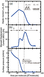
Figure 2. (a) Dipole moment of polar molecules estimated from MDC measurement. (b) MDC during monolayer compression. (c) Surface pressure-area isotherm during monolayer compression.
Download figure:
Standard image High-resolution imageSimilarly, we can sensitively probe the change of molecular forms such as cis–trans photo-isomerization induced in azo-benzene monolayers by alternating the photo-irradiation of ultra-violet and visible light [10, 13, 50, 51]. The trans- and cis-form isomers have the permanent dipole  and
and  (
( ), respectively. Accordingly, the MDC is generated during the photo-isomerization process. The detection of photo-switching due to cis–trans photo-isomerization in monolayers on solids as MDC signals will be available as a basic principle of organic memory elements as shown in figure 3, where alternating ultra-violet (UV) and visible (Vis) light irradiation results in the generation of alternating MDCs, whereas successive irradiation never generates a MDC [13, 51–53].

Figure 3. MDC due to photo-isomerization of azobenzene monolayer. The trans- and cis-conformation change of azobenzene induced the reversible MDC signals [13], copyright 1991 Nature Publishing.
Download figure:
Standard image High-resolution imageIt is instructive here to note that the surface potential measurement based on the Kelvin-probe method has been widely used for the study of monolayers at the air–water interface [54–56]. What we record by using this method is a compensation voltage  that is needed to make a zero-electric field between the monolayer and the suspended electrode. That is, a compensation voltage
  is applied to be
  in the surface potential measurement. By adding the contribution of
  to equation (1), we obtain the following equation:
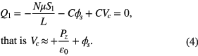
Here  is the dielectric constant of the air gap between the suspended electrode and monolayer, that is, nearly equal to the dielectric constant of vacuum. Equation (4) tells us that the conventional surface potential measurement probes polarization
  in accordance with the change of surface pressure by monolayer compression. In comparing equation (4) with equation (3), it is clear that the MDC measurement is very sensitive to the change of polarization
  with molecular area
  , while the surface potential measurement is not so sensitive. Actually it is very difficult to probe the change of polarization in the region before the initial rise of surface pressure by means of surface potential measurement. On the other hand, we can clearly see the generation of the MDC in this region, as shown in figure 2. Therefore, the MDC measurement has an advantage in probing dynamical dipolar motions in monolayers.
2.2. TOF measurement for probing electron and hole transport
As mentioned in section 1, in order to probe electron and hole transits across solids, time-of-flight measurement (TOF) is widely used [3–5, 9]. To clarify the difference between the TRM-EFISHG measurement and TOF, we briefly discuss the basic concept of TOF. Figure 4(a) illustrates the situation of the TOF measurement, where charge  is placed between two electrodes 1 and 2, separated by organic layer with a thickness of
  and connected to each other through an ammeter [5, 9]. Here this charge
  is displaced from electrode 1, and it is located at a distance
  from electrode 1. Owing to the neutrality of the charge of this electrode arrangement system, the electric flux density arising from charge
  converges on electrodes 1 and 2 as follows:

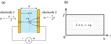
Figure 4. (a) The space charge  and induced charges
  and
and  on the electrodes. (b) TOF current that flows during transit of charge
  . The current flows only in the time 0 <
  <
<  .
.
Download figure:
Standard image High-resolution imageThe amount of induced charge  and
and  depends on position
  of charge
  . If charge
  moves at a constant velocity
  in the direction from electrode 1 to electrode 2, the amount of charge
  and
and  changes at a constant rate with time. Consequently, the constant current
  flows through the closed circuit whilst charge
  is being transported from the electrode 1 to electrode 2, as illustrated in figure 4(b). Transit time
  is given by
  , thus the total charge flowing through the circuit is
  . The current
  flowing through the circuit is generated due to the change of electric flux density between electrode 1 (or 2) and charge
  , and this is nothing but the MDC current. It is noteworthy that we here assumed that charge
  moves at a constant speed, thus it is possible to determine the position of the charge from the trace of the
  curve. However, if charge
  does not move at a constant speed, it is not easy to determine the position of charge
  by using the
  curve.
In the conventional laser-TOF measurement, we give a DC voltage  on electrode 2 with respect to the grounded electrode 1 to form a constant electric field
  between the two electrodes during the measurement [5, 17]. At
  , laser irradiation is employed to generate electron–hole pairs, only inside the organic layer near the electrode 1. Consequently, only electrons can move from electrode 1 to electrode 2 at a velocity of
  for
for  , whereas only holes can move from electrode 1 to electrode 2 at a constant velocity of
  for
for  . Here,
  and
and  are the electron mobility and hole mobility, respectively. Presumably we define the transit time by the relations
  (
( ) or
) or  (
( ), and we measure the carrier mobility of holes and electrons by changing the polarity of the applied voltage
  . This is the basic principle of the TOF measurement, and many experiments have been carried out for the determination of carrier mobility of polymers, insulators, organic semiconductors [5, 18], etc, since the pioneering work of the carrier mobility measurement on anthracene crystals by Kepler [17]. In actual experiments, however, there are many problems. For example it is very difficult to irradiate a laser beam around only electrode 1, in particular, in the case of very thin films. Also the space charge field caused by generated carriers distorts the electric field distribution in the system and the carrier transport will be thus governed by this electric field. Furthermore, there is an upper limit on the transit time that can be measured in the TOF measurement, namely the ohmic relaxation time of the film under test. That is, we cannot observe carrier transits in the region
  by using TOF if carriers decay with the ohmic relaxation time
  .
.
In the e-TOF measurement, the basic principle is the same as that used for the detection of MDCs. Instead of laser irradiation to generate electrons and holes, we apply a step voltage  to the two-electrode system to inject carriers from electrodes which transport between electrodes 1 and 2. As we probe the change of induced charges on the electrodes along with the transport of injected carriers, this idea is easily extended to a three-electrode case such as field-effect transistors [19–22], asymmetric needle-plane electrode systems [57] and others, although the amount of induced charge on the electrodes changes in a very complex manner, depending on the location of the charges. Figure 5 shows an example of e-TOF measurement that is carried out for the determination of hole mobility in pentacene by using pentacene field effect transistors [20]. As we can see in the figure, the transient current abruptly flows at around the time when the holes arrive at the counter (drain) electrode by crossing the channel. As shown in figure 5, e-TOF measurement is helpful for the determination of the carrier mobility of the materials, but it has a fundamental problem for usage. We cannot determine the polarity of the carriers merely from the trace of
  –
– curves, because positive and negative charges move along the electric field in opposite directions to each other. That is, the current is recorded as MDCs using an ammeter, but the MDC is proportional to
  =
=  and we cannot distinguish the polarity of charge carriers. Therefore, we need to determine the carrier polarity using other methods, before we carry out the e-TOF measurement. As mentioned above, the TOF measurement is helpful for the determination of carrier mobility, but this is under many physical boundary conditions.

Figure 5. TOF measurement of pentacene field effect transistors with various transistor channel length (L = 40, 50, 60, 80, 100 μm). In the measurement, holes are injected from the source electrode at t = 0, are transported across the transistor channel region, and arrived at the drain electrode at the time indicated by arrows. Reprinted with permission from [20]. Copyright 2009 American Chemical Society.
Download figure:
Standard image High-resolution image2.3. TRM-EFISHG for visualization of electron and hole transport
The basic concept of TRM-EFISHG is different from the TOF measurement, and this technique basically allows us to distinguish electron and hole transports. To understand the EFISHG, we again go back to Faraday's idea [1, 2, 23] formulated as the Gauss law. According to this law, the electric field arises from charges. We therefore postulate that solids surrounding electrons and holes can be polarized. Actually, in the presence of the non-zero DC electric field  by electrons and holes injected into organic solids, nonlinear polarization P is freshly induced, when laser light is irradiated on solids, owing to the interaction between the electromagnetic fields of the laser light and electrons in the organic materials. Figure 6 illustrates the basic principle of the EFISHG measurement [35, 36]. The non-zero DC electric field
  serves to distort the electron cloud of molecules. As a result, this kind of nonlinear polarization P is induced even in centrosymmetric molecular systems, such as pentacene, phthalocyanine, C60 and others [41, 58–61]. Induced nonlinear polarization P is given as

where  represents nonlinear optical susceptibility,
  stands for the angular wave frequency of the incident electromagnetic wave,
  and
and  represent the electric fields of laser, and
  is the static electric field arising from moving-carriers, which satisfies the relation [1, 2, 23]
where  is the charge density of the moving carriers, and
  and
and  are the relative permittivity of the organic materials and the absolute permittivity of free space, respectively. The induced polarization
  is a source of the second harmonic signal, and results in the enhancement of SH signal
  in proportion to the square of
  as
as

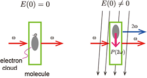
Figure 6. The generation of electric field induced optical second harmonic generation (EFISHG) light. In the presence of electrostatic field  , electron clouds in molecules are distorted and the nonlinear polarization P(2ω) is produced. As a result, EFISHG is emitted from molecules with intensity
  .
.
Download figure:
Standard image High-resolution imageHere  describes the SH intensity. From equations (7) and (8), it is clear that the distribution of SH intensity in solids changes in accordance with the electric field distribution, i.e. non-linear polarization distribution. Consequently, by using a time-resolved EFISHG technique, we can directly observe carrier transport in solids by monitoring the propagation of polarization
  induced in the solids along with carrier motion [24, 36]. It is noteworthy that in the EFISHG measurement laser irradiation is used to generate nonlinear polarization, and it can be postulated that no photo carriers are generated. This is because the basic second harmonic generation process is a two-photon process, and the EFISHG process is similar to this two-photon process [59]. Consequently, we can measure carrier transport in solids and others in a non-destructive way. This is the characteristic of the EFISHG measurement which differs from the laser-TOF measurement.
By the way, in electronic devices as well as in solids sandwiched between electrodes, there are many sources of DC electric fields. Among them are applying an external voltage, moving carriers, trapped charges, work function difference, and so forth. Consequently, the  in equation (8) is given by the sum of the electric fields from many sources as [4, 5]

Equation (7) with equation (8) suggests that we can probe electric fields  ,
, ,
,  and others by using the EFISHG measurement [29, 62–68]. The time-resolved EFISHG method is particularly helpful for probing carrier motion in solids, as described in section 3. It is noteworthy that
  is a material dependent parameter, and it specifies the feature of materials. As a result, the SHG is activated at a specific wave length
  (
( , speed of light) of the materials, and this fact allows us to selectively probe SHG generated from one layer of the multi-layers by choosing the laser wavelength appropriately [62, 69–71]. The magnitude of
  is very important in the EFISHG measurement. For example, the values of pentacene and C60 are in the order of 10−22 m2 V−2 (10−14 esu) at a laser wavelength of λ = 1120 nm and 10−18 m2 V−2 (10−10 esu) at λ = 1000 nm [72], respectively, and EFISHG signals generated by laser light irradiation from Q-switched YAG laser with energy of 1 mJ/pulse are probed as will be shown in section 4. Note that these
  values are large due to the resonant coupling between the laser beam and the electrons in the molecules [73].
It should be noted that there are many reports on SHGs since the pioneering works by Bloembergen [74] and Shen [59]. Those works focus on molecular structure and chemicals from viewpoints of spectroscopy for characterizing a material's structure. As a result, analysis of the SHG signal from non-symmetric chemical structures is the main topic. The SHG measurement employed in these works is different from the EFISHG measurement which we use here. Spectroscopic SHG experiments are carried out on focusing the SHG signal generated from materials in a form below,

where a main key parameter is the material dependent  parameter that depends on the arrangement of molecules and nonlinear susceptibility of molecules, but this is independent of the presence of the DC field,
  . This situation is very helpful to characterize material structures, e.g.
  = 0 for symmetric molecular systems, such as pentacene and C60. By choosing different light sources with wavelengths
  and
and  appropriately, the sum frequency generation method is carried out to precisely characterize material structures, the dynamical change of the orientational order of polar molecules, the interaction between molecules and surrounding solutions, and others (see text books [25, 59] and review papers [75–77]). However, this situation is quite different from the electric-field induced optical second harmonic generation (EFISHG) described by using equation (8), where the DC field
  makes a significant contribution by coupling with
  . In other words, EFISHG is not activated if
  Probing
  in equation (8) by means of EFISHG is indeed helpful for analyzing carrier behaviors and related electronic phenomena in organic devices. That is, we need to focus on the EFISHG process given by equation (8) to probe carrier motions and related electronic phenomena in electronic organic devices. As all electric phenomena have some relation with carrier behaviors, thus EFISHG provides a way for analyzing carrier behaviors in devices, e.g. organic field effect transistors, organic solar cells, organic light emitting diodes, organic memory devices, etc, and also for analyzing electric field distribution in organic materials, etc. In the following sections, we discuss the experimental systems and examples of EFISHG measurements.
3. Experimental system of EFISHG measurement
Figure 7(a) shows the basic arrangement of the experimental system used for the measurement of carrier transport, where the laser beam is vertically incident onto the sample through the objective lens, and the emerged SHG images from the samples are captured with time by using a CCD camera [24, 36]. The light source is an optical parametric oscillator, pumped by a third-harmonic light of Q-switched Nd:YAG laser (Continuum: SureliteII-10). To observe carrier transport, we need to construct an electrode arrangement appropriately. The most typical one is a planar type-OFET structure, where the source and drain electrodes are placed to be parallel on the organic semiconductor layer, and the gate electrode is placed on the substrate, as illustrated in the figure. Upon application of a step voltage, carriers are injected from the source or drain electrode into the organic semiconductor layer, and they are then transported along the channel, i.e. between the two electrodes. It is noteworthy that injection is dependent on the semiconductor materials and the electrode materials, but we can distinguish the carrier species, i.e. electrons or holes, by the SHG images [78–80]. The temporal resolution of the measurement system is limited by the pulse width of the laser and the rise time of the voltage pulse. Thus, the use of a short pulse laser such as femto- or pico-second lasers is effective to reduce the pulse width of the laser. On the other hand, there is further advantage of using short pulse lasers from the view point of nonlinear optical measurement. During the SHG measurement, we have to take care about the laser power to avoid damaging the sample. Sample damage is directly influenced by the pulse energy of the laser, not the instant optical power, whereas the SHG intensity is proportional to the instant optical power. Thus, the use of a short pulse laser is effective to observe the SHG signal without sample damage.

Figure 7. (a) The time-resolved microscopic SHG (TRM-SHG) measurement system that can visualize carrier propagation in organic field-effect transistors and others. As a light source, pulsed lasers such as Nd:YAG and femto laser are available. (b) Timing chart of DC voltage  and
and  , and pulsed laser incidence, for TRM-SHG measurements.
Download figure:
Standard image High-resolution imageEFISHG is activated from the organic semiconductor layer by choosing a fundamental laser wavelength appropriately. For example, 1120 nm was chosen for studying pentacene-organic field effect transistors (OFETs) [81–84]. The SH light generated from the semiconductor layer was filtered by a fundamental-cut filter and an interference filter to remove fundamental and other unnecessary light. Figure 7(b) illustrates an example of a timing chart of the laser pulse and step voltage applied to the OFET, which is used for the time-resolved EFISHG measurement. The parameter  stands for the delay time, and by choosing delay time
  we can visualize the carrier motions at time
  =
=  after applying the step voltage at
  = 0. That is, using the visualized images, the change of electric field distribution along the OFET channel, corresponding to the carrier transport, is probed with time. That means we can distinguish injected carriers, i.e. electrons or holes, from the visualized carrier motion.
At  = 0, upon application of a step voltage, the carrier injection starts with no carrier injection into the semiconductor layer, while at
  =
=  the injected carriers distribute along the channel of the OFETs [85–88]. That is, we can directly visualize the electric field distribution formed in the OFET only by external voltages by choosing
  = 0, whereas we can map the injected carrier distribution with time by choosing
  .
.
It is noteworthy that the EFISHG experiment is employed in the same way for sandwiched-type devices with two electrodes, by using a laser beam that is obliquely incident onto the devices [28, 89–92]. Further, we have recently developed a novel method that can detect an electric field along the direction of the incident laser beam by introducing a radial polarized beam into the EFISHG measurement system, and this system also makes it easy to study carrier transport in sandwiched-type devices [93, 94].
One may have concerns about the generation of photo-carriers by the irradiation of laser pulses that possibly affect the electrical properties of the material. As mentioned, this can be neglected because the wavelength of the fundamental light is far from the absorption peak. However, to satisfy the resonant condition, the photon energy of SH light should be close to the optical gap. Then we still need to take into account the photo-carrier generation by the two-photon absorption. Here we discuss the effect of two-photon absorption in C60 as an example. The two-photon absorption coefficient β of C60 was reported as 40 cm GW−1 at a wavelength of 1064 nm [95]. Assuming a typical Q-switched YAG laser with energy of 1 mJ/pulse and a spot size of 1 mm, a peak power of the pulse is roughly estimated as 0.02 GW cm−2. These parameters are substituted into  to evaluate the loss of optical power due to two-photon absorption after passing through the C60 film with a thickness d of 100 nm. Then, we obtain
  . Accordingly, we neglect the effect of photo-carrier generation in the EFISHG measurement.
4. EFISHG Measurements and Modelling of Carrier Behaviours
4.1. Carrier distribution and carrier motion
As described in section 2.3, we can measure electric field distribution in organic devices, carrier motion in organic devices, and others by probing non-linear polarization that results in EFISHG images. Firstly we discuss some examples and then discuss how carrier behaviors are modeled on the basis of experimental results.
4.1.1. Stationary-state.
Since the discovery of conducting organic materials, organic devices have attracted much attention in electronics. Among them are organic light emitting diodes, organic field effect transistors, organic memory devices and so forth. In these electronic devices, organic semiconductors are used as active layers to realize their own device function, on the basis of general semiconductor device physics [96]. However, the carrier injection and transport mechanisms in actual organic devices are not so simple, owing to the dielectric nature of active organic layers. Basically, intrinsic carrier density is quite low in active organic layers. As a result, carrier injection process makes a dominant contribution. We can see such examples in organic field effect transistors and organic light emitting diodes, whose device performance are governed by the carrier injection process. This situation is very similar to the carrier transport in dielectric materials. Accordingly, it is a very effective way to directly measure electric field distribution changes in active layers in these organic devices for analyzing and modeling carrier behaviors. This is a dielectric physics approach that is helpful for analyzing carrier injection and transport of dielectric materials [4, 5, 9]. As already described in section 2, EFISHG measurement is capable of detecting an electric field formed in organic devices due to static electric fields by an external applied DC voltage and time-varying electrostatic field by injected carriers. Keeping in mind this idea, the electric field distribution formed along the channel of pentacene-OFETs has been measured. The electric field distribution formed in the pentacene-OFETs before and after hole injection into the channel has been well explored [81, 97], and the electric field distribution before hole injection is shown to be in good agreement with the distribution analyzed using the rigorous solution of the Laplace field of the electrode system of OFETs [98, 99]. Furthermore, the electric field distribution originated from injected carriers has been determined from the EFISHG measurements, and it has been shown that the charge distribution along the OFET channel is basically determined based on a Maxwell–Wagner model that accounts for carrier accumulation at the interface between the gate-insulator/active organic layer interface [98–101].
Figure 8 shows a typical example of the EFISHG measurement carried out for top-contact pentacene OFETs with Au source and drain electrodes [98]. Under the condition of no carrier injection of the OFETs, EFISHG is shown to be activated to satisfy the rigorous solution of the Laplace equation of a three-electrode system of the OFETs [98, 99], as shown in figure 8(a). On the other hand, under the condition of hole-injection, the intensity of EFISHG decreases due to the space charge field formed along the channel by injected holes, as shown in figure 8(b) [97, 99]. Using equations (8) and (9), the carrier distribution along the channel is determined using the EFISHG measurement, as plotted in figure 8(b). These results show that carrier accumulation along the channel is governed by the Maxwell–Wagner effect, and the distribution is basically determined based on a Maxwell–Wagner model [84, 102, 103]. Our further EFISHG study shows that the carrier distribution along the channel in the steady-state that follows a solution of a classical differential equation of current that describes the continuity of carrier transport along the channel, which is modeled based on a transmission line model, as an extension of the Maxwell–Wagner model [100, 104]. Analytical results show that the potential distribution along the channel is not linear, but it changes on satisfying the square root dependence along the channel, as [100, 104]
where  and
and  represent the edge of the source and the drain electrodes, respectively. Accordingly, the electric field distribution is given as

Figure 8. (a) The electrostatic field (Laplace field) formed in the pentacene field-effect transistor. The black curve is the electric field distribution which was directly visualized by TRM-SHG measurement. The thick gray curve is a numerical calculation by a finite element method. Reprinted with permission from Yamada et al [98]. Copyright 2008, AIP Publishing LLC. (b) The electric field distribution at the drain electrode edge of the pentacene field-effect transistor. The filled circles and open squares plot electric field distributions with and without hole injection, under DC voltage application to the gate electrode with reference to the Au Source electrode ( < 0). Reprinted with permission from Yamada et al [99]. Copyright 2008, AIP Publishing LLC.
Download figure:
Standard image High-resolution imageEFISHG probes this electric field distribution well, and generates the signals that follow equation (8) with equation (12), where  of equation (8) is replaced by the
  of equation (12).
As described above, it is clear that EFISHG is available for probing the steady-state carrier distribution along the channel of OFETs. By the way, some organic materials show ambipolar behavior, which means that electrons and holes are allowed to enter into materials from the electrodes. In the field of electrical insulation engineering, this carrier behavior is called double-injection [4]. Consequently probing electron and hole injection, and their distribution in organic devices is also important. For example, for organic light emitting device application, double carrier injection, i.e. electron and hole injection, is a key for device operation. Using ambipolar organic light emitting transistors (OLETs) with an active layer of the green-light-emitting polymer of poly(9,9-dioctylfluorene-alt-benzothiadiazole)(F8BT), which has a photo luminescent peak at a wavelength of 560 nm, the EFISHG measurement has been employed using a laser beam with a wavelength of 840 nm [79, 101]. Of course, for the EFISHG experiment, we need to remove the influence of photoluminescence, by using a band pass filter so that we can probe the EFISHG that is generated at a wavelength of 420 nm only. The EFISHG experiments showed that there is actually a zero-potential position in the channel, which corresponds to the meeting point of electrons and holes for the electroluminescence [101].
4.1.2. Transient carrier behavior.
As mentioned in section 2, it is possible to probe carrier motion by means of the TRM-SHG. Using the electrode system illustrated in figure 7, i.e. top-contact pentacene FETs with a Au source and drain electrodes, TRM-SHG measurement has been carried out using OFETs with a channel length of 40 µm. Here the pentacene was deposited at room temperature, i.e. around 20 °C. Figure 9(a) shows the TRM-SHG image in the channel region of the pentacene FET with a 500 nm thick SiO2 gate insulator, where the SHG image was obtained along with carrier motions after a step positive voltage was applied. That is, a positive voltage Vpulse = 70 V was applied to the source electrode with respect to the gate and drain electrodes that were electrically shorted and grounded, i.e. Vds = Vgs = −70 V. At  = 0 ns, the laser pulse coincides with the rising edge of the voltage pulse, and SHG signals are found near the edge of the source electrode, indicating the Laplace electric field E0, parallel to the channel, is formed only around the source electrode. Interestingly, as is clearly shown in the image, the emission band of the SHG signal gradually moves in the channel from the source to drain electrode. The visualized emission band motion, which starts from the source electrode, evidently indicates hole-injection from the Au-source electrode. That is, the pentacene FET shows a p-type semiconductor behavior, where the majority of carriers are holes injected from the source electrode and the carrier mobility is 0.1–0.2 cm2 V−1 s−1. Note that the SHG image appears only in the region within a radius of around 150 µm, owing to the spot size of the laser (see the region indicated by a circle in figure 9(a)). To further clarify the hole transport mechanism across the channel, we plotted the SHG peak position with respect to elapsed time, as shown in figure 9(b) [37, 82, 105]. From figures 9(a) and (b), it is clear that holes travel in the direction from the source Au electrode to the drain electrode, on satisfying the square root time dependence [105, 106]. This time dependence reflects the interface charge propagation process (see figure 9(b) and [100, 107]), and well supports a Maxwell–Wagner effect model that is employed for analyzing transient carrier behaviors along the OFET channel. This is also well supported by a transmission line model that is basically based on the extension of the Maxwell–Wagner model. In physics, carriers propagate along the interface between the gate insulator and active layer, and this situation is roughly described as the interface accumulated charge,
  , spreads with a velocity of
  , and is thus illustrated by using a RC ladder circuit [100]. Here
  is the gate capacitor and
  is the threshold voltage.
  is the applied gate-source voltage and
  is the applied drain-source voltage and
  (
( ) is the average voltage for carrier drift in the FET channel region. In more detail, the transit time
  is approximately given by [100]
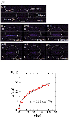
Figure 9. (a-1) The TRM-SHG image of holes propagating in the pentacene field-effect transistor. The top and bottom region of the image are the drain and source electrodes, while the center region is the transistor channel (L = 40 μm). Upon voltage application to  (<0) at τ = 0 s, holes are injected from the source electrode edge to the channel. (a-2)–(a-7) The EFISHG images visualize the injected holes propagating to the drain electrode. The carrier front of the holes, indicated by arrows, shift from the source to the drain as the time τ elapsed after DC voltage application. (b) The motion of carrier front position from the source electrode edge. Holes propagate along the transistor channel on satisfying the
  relation, indicating that carrier drifting governs the carrier transport mechanism [37].
Download figure:
Standard image High-resolution imageHere  is carrier mobility, and
  is channel length. Equation (13) suggests that the carrier migrates into the channel region on satisfying the square root time dependence. The computer simulation based on a classical drift-diffusion equation supports this prediction [106–109].
On the other hand, under the application of a negative step voltage, the position of the SHG peak does not move, and the SHG signals are only concentrated around the edge of the source electrode during the measurement. Results suggest that electron injection is minor and this process is negligible [26, 110].
By the way, carrier injection is governed by the electrode materials and semiconductors. Accordingly the film preparation condition is very important, and we can prepare pentacene layers that exhibit ambipolar behavior by controlling the substrate temperature during the deposition of the pentacene layers. Figure 10(a) shows the  –
– characteristics of pentacene FET with a 500 nm thick SiO2 gate insulator, where the pentacene film was deposited at a substrate temperature of 70 °C and the channel length is 50
  . An ambipolar behavior is seen in the
  –
– characteristics. That is, both electrons and holes serve as carriers, depending on the applied
  . By employing the TRM-SHG experiment, we get the relationship between the position of the carrier front with elapsed time by applying the step voltage
  . The results show that the hole mobility is much higher than the electron mobility, i.e. about 100 times higher, as portrayed in figures 10(b) and (c) [111]. With consideration of these results, we can visualize the double carrier injection process that leads to recombination between electrons and holes injected from the source and drain electrodes. Figure 11 shows the TRM-EFISHG experiment, where a negative step voltage of Vdg = −100 V was applied on the drain electrode with respect to the gate, and at the same time a positive step voltage of Vsg = +100 V was applied on the source electrode. As can be seen in the images of figure 11, double carrier injection followed by the electron–hole recombination is clearly demonstrated. At the time corresponding to carrier recombination, a bright band is seen due to the formation of a high electric field between the electrons and holes injected into the channel from the drain and source electrodes, respectively.
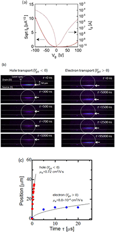
Figure 10. (a)  –
– curve of the ambipolar pentacene field-effect transistor. Reprinted from Manaka et al [170]. Copyright 2011, with permission from Elsevier. (b) TRM-SHG images directly visualizing hole (left) and electron (right) transport in the ambipolar pentacene field-effect transistor. Holes and electrons are injected from the source electrode edge by the voltage application
  < 0 and
  > 0, respectively. The carrier propagating front, indicated by arrows, shift from the source to the drain as the time τ elapsed. (c) Time dependence of the carrier front position from the source electrode edge, for holes and electrons moving in the pentacene OFET channel.
Download figure:
Standard image High-resolution image
Figure 11. TRM-SHG measurement of ambipolar pentacene OFET. (a) SHG image visualizing carrier motion of both holes and electrons. (b) Experimental setup for pulse voltage application to OFETs. Electrons were injected from the drain electrode prior to hole injection from the source electrode. (c) SHG intensity profile across the OFET channel from the source electrode edge (0 μm) to the drain electrode edge (45 μm). The SHG peak corresponding to the frontier where propagating holes meet electrons at around 33 μm. The enhanced local electric field due to the hole–electron recombination process is clearly observed in the bottom profile (400 ns).
Download figure:
Standard image High-resolution imageAs shown in figure 11, the TRM-EFISHG measurements allow us to visualize the double carrier transport process, i.e. double carrier injection and recombination. Consequently, this technique is available for studying the electro-light emitting process that starts from double carrier injection leading to carrier recombination, and also for visualizing the process that leads to the pre-electrical breakdown in devices.
Further we should note that carrier propagation is dependent on the interfacial film condition of the channel, e.g. carrier traps, morphology, etc. Equation (8) with equation (9) suggests that TRM-SHG is available for monitoring the contribution of the surface states of the channel. To confirm the potentiality of the TRM-SHG measurements, similar experiments were carried out for pentacene-FETs with a 100 nm thick poly-methylmethacrylate (PMMA) layer on the surface of the gate SiO2 insulator [112, 113]. The SHG intensity is concentrated in the front region of the propagating SHG profile [112]. Results indicate that the space-charge field distribution is being formed along the channel due to the trapping of holes. Analysis based on a carrier trap model accounts well for the TRM-SHG experiments. That is, TRM-SHG is effective to probe the interface states of the channel region.
It is also noteworthy that the activation of EFISHG is material dependent, due to the material dependent parameter  with angular frequency
  in equation (8). Consequently, probing carrier motion in one of the layers in multi-layer systems is possible. Actually, we have already demonstrated the detection of such carrier motions in OFETs with an active layer of double-layer system, e.g. OFETs with a C60/pentacene active layer, etc [71, 114, 115], where the hole carrier transport in the pentacene layer and electron carrier transport in C60 were selectively probed by choosing appropriate wavelengths of incident laser, which activate pentacene at 1120 nm and C60 at 1000 nm, respectively. That is, we can directly probe carrier motions in one of the multilayers by choosing an appropriate incident laser wavelength. The EFISHG measurement for pentacene/C60 OFETs showed that electrons are actually transported in the C60 layer, etc.
4.1.3. Anisotropic carrier behavior.
Carrier transport is strongly dependent on the film preparation condition, crystallinity of deposited films, and so forth. There are many film preparation methods, such as dipping, spin-coating, evaporation, and others. Accordingly the anisotropic property is induced in deposited films, and the organic film shows the anisotropic carrier transport property; carrier transport along the long-molecular axis direction is different from transport perpendicular to the long-molecular axis direction. Evaluating the anisotropic carrier behavior is very important for device technology, and also for understanding the carrier transport mechanism. By using the TRM-EFISHG measurement, we can visualize the anisotropic carrier transport behavior in organic thin films by using a round shape electrode system [116]. Figure 12(a) shows the visualized SHG images by holes into poly[(9,9-dioctylfluorenyl-2,7-diyl)-co-bithiophene]) (F8T2)-films from the edge of the round shape Au electrode. Here the F8T2 films were prepared using the floating film transfer method (FTM). As we can see in the set of figures (see figures 12(a-1)–(a-3)), the spreading speed of holes from the edge of the round shape electrode is totally directional dependent on the film. As we can see in the distorted SHG image of injected holes around the Au edge of electrode, carrier spreading is seen along the FTM direction, i.e. parallel to the molecular long-axis direction of F8T2. On the other hand, the visualized carrier behavior of holes in pentacene films deposited by thermal evaporation is isotropic, as shown in figures 12(b-1)–(b-3). In this way, we can evaluate the anisotropic carrier behaviors by using the TRM-EFISHG microscopic images [116, 117].
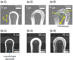
Figure 12. (a-1)–(a-3) The anisotropic hole transport in F8T2 film prepared by the FTM method. The holes are injected from the round-shaped single electrode, and transported in the film with maximum carrier mobility  and with minimum carrier mobility
  as illustrated. EFISHG images clearly suggest that hole mobility is high in the FTM direction (indicated by an arrow in (a-3)), reflecting anisotropic F8T2 film formed by the film preparation process.
  in (a-1) indicates the polarization direction of the incidence laser beam. (b-1)–(b-3) The isotropic hole transport in pentacene film prepared by conventional vacuum evaporation. TRM-SHG visualized the isotropic carrier transport of the pentacene film, reflecting isotropic morphology of the pentacene film by vacuum evaporation.
Download figure:
Standard image High-resolution image4.2. Carrier motion in sandwich-type devices
As mentioned in section 2, EFISHG measurement is available for measuring electric fields in the film thickness direction as well as for probing carrier motions in sandwiched-type devices, most conventionally by introducing incident laser light obliquely onto such devices [28, 90, 118–121]. Here we discuss topics related to the detection of electric field and carrier motions in the film thickness direction.
Sandwich-type devices such as organic light-emitting diodes (OLEDs) and organic solar cells (OSCs) are designed on the basis of general semiconductor device physics. However, owing to the dielectric nature of organic semiconductor layers, the complexity of interfaces, the presence of traps, etc, it is quite a task to describe the energy diagram of actual organic devices. For example, organic double-layer diodes comprised of p- and n-type organic semiconductors show a rectification property, but the actual potential distribution formed in these diodes is far different from the general semiconductor p-n diodes, owing to the dielectric nature of the organic semiconductor layers [89]. Consequently, it is very effective to directly measure the electric field and potential distributions in these devices for analyzing carrier behaviors in actual organic diodes [28, 122]. We encounter a similar situation when we talk about the rectification properties of MIS diodes using organic semiconductor layers [123, 124]. As already discussed, EFISHG can directly and selectively probe the electric field distribution in one of the organic layers, and this technique also enables us to study carrier behaviors in organic sandwich-type devices [125–127]. The results of EFISHG are very helpful for determining the rectifying property of organic double-layer diodes, e.g. diodes with a structure of ITO/PI/TIPS-pentacene/Au [128, 129].
4.2.1. Double layer EL diodes.
OLEDs have attracted much attention in electronics. Basically, an OLED is an injection-type device with two different electrodes that are separated by an organic multilayer [130]. Using an energy diagram of the molecules, e.g. HOMO and LUMO states, (highest occupied molecular orbital and lowest unoccupied molecular orbital, respectively) much research has been carried out for improving device performance [131]. Ideas of using low work function electrodes, depositing dipolar layers on the surface of electrodes, utilizing multilayer systems comprising hole- and electron-transport, electroluminescent layers, and so forth have been presented [131, 132]. These important ideas are well accepted to achieve high-performance OLED devices [133]. However, owing to the ambiguities of energetics at the organic-metal and organic-organic interfaces, the carrier behavior in OLED devices is still not fully understood. To clarify the details, we need to pay attention to carrier injection from electrodes, carrier transport across active layers, and charge accumulation and recombination at the interface which lead to electroluminescence (EL). Hence, one of the most effective ways is to directly probe carrier motion in OLED devices. Probing carrier behaviors in combination with charge accumulation at the interface is particularly important, because the Maxwell–Wagner effect suggests carrier accumulation at the interface of layers, and this accumulation contributes to form the space charge field. Consequently, EFISHG measurement coupled with the Maxwell–Wagner model analysis is very helpful for this purpose [28, 29, 89, 134, 135]. Making use of the TRM-EFISHG experiments on double layer OLEDs with N,N'-di-[(1-naphthyl)-N,N'-diphenyl]-(1,10-biphenyl)-4,4'-diamine ( -NPD) and tris (8-hydroxy-quinolinato) aluminum(III) (Alq3) layers by applying a step voltage showed well the charging and discharging of carriers on electrodes and carrier transit across the
  -NPD and Alq3 layers, and the non-reversal charging and discharging processes resulted from the different carrier behaviors accompanied by ordinary green EL [29, 89].
To analyze carrier behaviors of OLED devices, EFISHG measurement is carried out by laser irradiation with a wavelength of 820 nm, in order to selectively measure the electric field formed in the  -NPD layer by probing the SHG
  with a wavelength of 410 nm [28]. Upon application of the external voltage
  , the electric field across the
  -NPD layer
  varies with time, on satisfying the following relation:
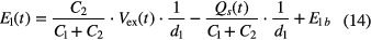
Here  and
and  are the capacitance of the
  -NPD layer and Alq3 layer, respectively,
  is the thickness of the
  -NPD layer.
  is the electric field caused by the work function difference etc, which corresponds to other terms in equation (8).
  is the interface charge accumulated at the interface between
  -NPD and Alq3 layers owing to the Maxwell–Wagner effect. The EFISHG is given by equation (8) with
  of equation (14), instead of
  . That is, the generated EFISHG changes on satisfying equation (14), showing that interface charge
  is accumulated with a response time governed by the Maxwell–Wagner relaxation time.
Figures 13 and 14 show, respectively, EL and EFISHG measurements under application of an AC square voltage to the ITO/ -NPD /Alq3/Al OLEDs [136, 137]. Two kinds of AC square voltage waveforms are chosen, one with no DC components (square voltage a), and the other with DC components (square voltage b). As figure 13 shows, EL is generated in accordance with the applied AC square voltage, where the generation is dependent on the applied frequency and also the waveform. In more detail, the EL intensity gradually decays with the increase of the frequency of the applied AC square voltage, and reaches a minimum at the frequency corresponding to the carrier transit time of the Alq3 layer. Interestingly, the EL intensity again increased by the application of further higher frequency AC square voltages, relying on the DC component of the AC square voltages [138–140]. Results suggest the presence of two EL modes, where the space charge field caused by the interface charge makes a significant contribution. That is, in the low frequency region, accumulated holes at the interface suppress hole injection and lead to the decrease of the EL intensity activated by the recombination of holes and electrons injected from opposite electrodes. On the other hand, in the high frequency region the accumulated holes assist electron injection and result in the increase of EL intensity activated by the recombination of the interfacial accumulated holes and injected electrons from Al electrode. However this is merely speculation, and we need to make clear the presence of this space charge field caused from accumulated interface charges and its contribution. For this purpose the EFISHG measurement is useful. Figure 14 shows the EFISHG measurements in the low frequency region, where two kinds of AC square voltage waveforms are chosen, i.e. one with no DC component (square voltage a), the other with a DC component (square voltage b) [136–138]. From the top to bottom, the applied external voltage,
  , generated EFISHG intensity
  , electric field
  and accumulated interface charge
  are plotted. Here the generated EFISHG intensity
  is plotted by
  with consideration of the relation between the electric field and the generated EFISHG (see equation (8)).
  is calculated using the Gauss law of equation (7) with the EFISHG equation (8). Under the AC voltage application with no DC component (square voltage a), in region A,
  is zero, in prior to voltage application
  = +20 V. In region B, external voltage
  = +20 V induces charges on the ITO and Al electrodes with a circuit response time
  (
( )
)  10−7 s, and forms an electric field in the α-NPD layer as high as
  5.6 × 10⁵ V cm−1. After that, in region C, holes are injected from the ITO to α-NPD layer and electrons are injected from the Al to Alq3 layer for radiative EL recombination. The holes smoothly transport in the α-NPD layer (hole mobility:
  10−4 cm2 V−1s−1) but electrons go through the Alq3 layer slowly (electron mobility:
  10−5 cm2 V−1s−1), due to the imbalance of hole and electron transport in the layers. As the result, holes accumulate excessively at the α-NPD/Alq3 interface, and the electric field in the α-NPD layer decreases. The EFISHG shows that the electric field actually decreases from
  5.6 × 10⁵ V cm−1 to
  4.8 × 10⁵ V cm−1 at
  10−5 s due to excess hole accumulation
  6.5 × 10⁻⁸ C cm−2.On the other hand, under AC voltage application with a DC component (square voltage b), electrode charges are induced on the ITO and Al electrodes and holes accumulated excessively at the α-NPD/Alq3 interface, in a way similar to the carrier processes under the square voltage a. However, excess holes stay at the α-NPD/Alq3 interface in regions A and E
  = 3.0 × 10⁻⁸ C cm−2, as evidenced by the EFISHG measurement. These results support the prediction that there are accumulated holes at the interface, and these charges suppress hole injection in the low frequency region and lead to the decrease of the EL intensity. Using the EFISHG results, we can carry out a similar discussion on the presence of interface charge and its contribution, in terms of the EL in the high frequency region [137, 140]. In this way, we can monitor dynamical carrier behaviors in charging and discharging processes in EL devices, by means of EFISHG.
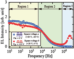
Figure 13. EL intensity curve as a function of frequency of square wave voltage. The blue squares show EL under voltage with no DC component (square voltage a), while red circles plot EL under voltage application with a non-zero DC voltage component (square voltage b).
Download figure:
Standard image High-resolution image
Figure 14. EFISHG measurement of an ITO/α-NPD/Alq3/Al double-layer OLED, under application of voltage with and without a DC component. (a) Square-root of the SHG intensity  . (b) Electric field in the α-NPD layer estimated from the SHG intensity. (c) Interfacial charge
  accumulating upon voltage applications.
Download figure:
Standard image High-resolution imageIt is noteworthy that electroluminescence has received much attention as one of the pre-breakdown phenomena in the field of electrical insulation engineering for the past decade, where the main research interest is to detect very weak EL signals for the diagnostics of insulators. However, using EFISHG provides a new way for the detection of the pre-breakdown phenomena because carrier motions leading to carrier recombination can be monitored, as shown in figure 15 [141].
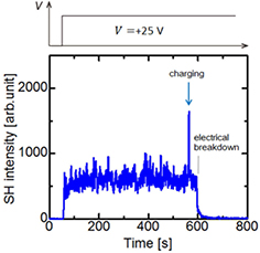
Figure 15. EFISHG-t measurement that detects instantaneous charging of OLED (device structure: IZO/α-NPD/Alq3/Al) as a pre-electrical breakdown phenomena. Results showed that (1) SH intensity is stable after DC voltage was applied to OLED at t = 50 s, (2) SH intensity occasionally and instantaneously enhanced due to charging prior to electrical breakdown at t = 560 s, as indicated by an arrow, (3) electrical breakdown occured at t = 600 s. In the measurement, the electric field in the α-NPD layer was probed for detecting pre-electrical breakdown phenomena, by using the probing laser beam with a wavelength of 820 nm.
Download figure:
Standard image High-resolution image4.2.2. Double layer memory devices.
Ferroelectric polymers are widely used as memory materials, where the copolymer of vinylidene fluoride (VDF) and trifluoroethylene (TrFE), P(VDF-TrFE) stands out as its bistable and remanent polarization can be repeatedly turned-over by an external electric field [142, 143]. Recently, ferroelectric polymers have also been used in electronic devices such as organic field effect transistors (OFETs) [144, 145] and organic photovoltaic cells (OPVs) [146, 147], where a strong internal electric field induced in the active layer of these devices by spontaneous polarization of ferroelectric polymers is well utilized for efficient device operations. As a result, carrier behaviors in the active semiconductor layer, e.g. pentacene, have been deeply studied in terms of the turn-over of the spontaneous polarization of ferroelectric layers [148, 149]. For p-type pentacene OFETs with a ferroelectric P(VDF-TrFE) gate insulator, hole/electron injection, transportation, charging, and discharging at the P(VDF-TrFE) gate insulator interface and so forth have been clarified in response to the turn-over of spontaneous polarization of the ferroelectric layer. Similarly, organic memory MIS diodes with a ferroelectric P(VDF-TrFE) insulator have been studied. These studies are mainly carried out by means of electrical measurements such as displacement current measurement (DCM) using a ramp voltage [150, 151], but these are no longer sufficient to account for carrier behaviors in a variety of organic semiconductor devices being utilized with ferroelectric P(VDF-TrFE) layers. Using EFISHG probes, the electric field change induced in organic devices with a ferro-electric layer gives much information on the carrier behavior in these devices [152–154].
Figure 16 shows a typical example of DCM measurements for metal-ferroelectric layer-metal (MFM) and metal-ferroelectric layer-semiconductor-metal (MFSM) (the inset of figure 16(a)) devices, which were prepared on patterned indium zinc oxide (IZO) substrates [30]. A P(VDF-TrFE) (VDF:TrFE = 72: 28 mol. %) layer with a thickness of 200 nm was spin-coated on the substrate, and then a pentacene layer (200 nm, for the MFSM device) and gold electrode were thermally evaporated successively. For the DCM measurement, a ramp voltage was applied on the IZO electrode. Figure 16(a) shows the results of the DCM for the MFM device. Two peaks (peaks A and B) are clearly observed at symmetric positions at voltages corresponding to the coercive electric field  of 0.6 MV cm−1, and show no dependence on the sweeping frequencies of the ramp voltage. These results suggest that the appearance of peaks A and B are due to the turn-over of spontaneous polarization.

Figure 16. Displacement current measurement of organic memory devices under triangular voltage application. (a) MFM structure device (IZO/P(VDF-TrFE)/Au). (b) MFSM structure device (IZO/P(VDF-TrFE)/pentacene/Au. Reprinted with permission from Li et al [30]. Copyright 2011, AIP Publishing LLC.
Download figure:
Standard image High-resolution imageOn the other hand, for MFSM devices, three peaks A, B, and C are clearly observed. The appearance of the third peak, peak C, at the non-symmetric position of peak A is a typical characteristic of the MFSM device. Results suggest a two-step polarization reversal of the ferro-electric layer in the pentacene/P(VDF-TrFE) double-layer device. However this is merely speculation. For studying carrier behaviors with the turn-over of polarization, it is very helpful to measure the electric field formed in pentacene and P(VDF-TrFE) layers. Figure 17 shows the result of EFISHG measurement, where the electric field across the pentacene layer is recorded [31]. Results clearly verify the proposed two step polarization reversal process by the two different hysteresis loops: one loop is in figure 17, corresponding to peak A and B, and the other loop corresponding to peak C [148]. Results of EFISHG suggest that the interaction of interfacial charge and ferroelectric polarization is responsible for this two-step process. It is noteworthy that the situation of the 2-step turn-over strongly depends on the organic semiconductor materials, where the interaction at the interface between the ferroelectric layer and semiconductor layer is quite different. For example, for P(VDF-TrFE) /C60/Au (or Al) double layer devices, only two peaks appear, but the peak position appears at quite different voltages from those of the P(VDF-TrFE) /pentacene /Au double layer device, owing to the potential drop across the C60 layers. Using the EFISHG measurement is an effective way for clarifying the contribution of organic semiconductor layers [153, 155].

Figure 17. EFISHG measurement of the MFSM type memory device. The result shows the hysteresis behavior of the memory device. Loop 1 is the first-step polarization reversal of peak B in the DCM, while loop 2 is the second-step polarization reversal of peak C. (a) Electric field change estimated based on the Maxwell–Wagner effect model. (b) Electric field directly probed by the EFISHG measurement. Reprinted with permission from Li et al [31]. Copyright 2012, AIP Publishing LLC.
Download figure:
Standard image High-resolution image
4.2.3. Organic solar cells.
There are many kinds of organic solar cells (OSCs), e.g. bilayer type, blended-type, etc. Among them the bulk hetero-junctions (BHJs) OSCs have been paid much attention in terms of the conversion efficiency of OSCs. Using BHJs, an idea for the introduction of hole and electron blocking layers has also been developed. However the basic mechanism of carrier behavior is getting more and more complex. Thus the development of techniques available for probing carrier behaviors in OSCs is anticipated, for getting the whole picture of carrier behaviors.
In BHJs OSCs, electron donor and acceptor molecules are mixed to introduce a larger contacting area for creating excitons to be separated into electrons and holes efficiently. However the identification of carrier paths is very speculative in such devices. The EFISHG measurement is very useful to investigate fundamental processes, not only in bilayer (double active layer) OSCs but also in blended-type OSCs [156–160]. The main reason is that the generation of the EFISHG depends on the material properties of the targeted sample. Consequently, it is possible to observe and study different material components in the BHJ layer individually, by choosing two appropriate laser wavelengths. This is an advantage of EFISHG for the study of carrier path in BHJ OSCs. For example, for OSCs co-deposited with pentacene and C60, EFISHG measurement has been carried out at two laser wavelengths of 1000 nm and 860 nm, by which carrier behaviors inside the pentacene and C60 have been selectively probed. As a result, the presence of two carrier paths for electrons and holes has been identified from the EFISHG response by application of a laser pulse to the OSCs [63]. The EFISHG provides an additional promising method to study the carrier path of electrons and holes as well as dissociation of excitons in BHJ OSCs [161, 162]. Furthermore, recently much attention has been focused on perovskite solar cells, where the dissociation of excitons is postulated to happen in the bulk of the solar cells. We believe that EFISHG can be employed to make clear the contribution of the internal electric field, and thus the technique is available for studying the carrier process.
As mentioned above, EFISHG is available for studying carrier behaviors in organic devices. Finally we should note that this method has a potentiality to study carrier behaviors in inorganic devices, such as amorphous silicon (a-Si) solar cells [163] and AlGaN/GaN high electron mobility transistors (HEMT) [164, 165].
5. Conclusions
In this review paper, we summarized novel methods for studying carrier motions in solids and in devices by probing polarization induced in organic materials. The methods are Maxwell-displacement current (MDC) and electric field induced optical second harmonic generation (EFISHG) measurements. In both measurements, polarization is a key parameter for the detection of dynamical carrier motions. In the MDC measurement, we probe polarization induced by orientationally aligned dipoles, by measuring the change of induced charge on electrodes with time. On the other hand, in the EFISHG measurement, nonlinear polarization induced in solids in the presence of a DC electric field is probed by coupling with a laser beam. As carriers are sources of electric fields, we anticipate that EFISHG is broadly available for studying electronic devices. As mentioned above, by focusing on polarization induced by dipoles, and electrons and holes, we find a way to analyze dynamical carrier motion in solids and in devices. In the future, we also need to study a way for probing dynamical motions caused by quadrupoles and others. Further, we need to couple MDC and EFISHG measurements with other methods that can probe carrier motions in energy space. The coupling of charge modulation spectroscopy, electro-absorption spectroscopy, and others will be effective [115, 166–169]. Further experiments and studies proceed.
Acknowledgment
A part of this work was financially supported by a Grant-in-Aid for Scientific Research (Nos. 01550239, 22226007, 24360118, 25709022, 22760227) from the Japan Society for the Promotion of Science.