
ABSTRACT
Microlens arrays are now widely used in a variety of astronomical instruments that require high performance. This paper describes the applications of microlenses in astronomical spectroscopy and discusses the necessary performance requirements. A variety of optical tests, including high dynamic range point‐spread function measurements and determination of encircled energy, were developed to characterize the performance of a variety of lenslet arrays. Results are presented that indicate the best types of lenslet array for use for astronomical spectroscopy.
Export citation and abstract BibTeX RIS
1. INTRODUCTION
The use of arrays of small lenses in astronomical instrumentation is now becoming widespread. Traditionally, microlenses have been used by astronomers for wave front sensing in adaptive optics systems (e.g., Artzner 1998). In general, wave front sensing requires lenses with large focal ratios and small aperture. Lenses such as these are straightforward to manufacture and can be obtained with excellent quality. More recently, the use of lenslet arrays in instruments to perform astronomical spectroscopy has become common. Spectroscopy is very demanding on microlens performance, requiring large‐aperture fast lenses; hence the importance of developing accurate microlens testing techniques.
This paper will concentrate on the characterization of lenslet arrays for use in astronomical spectroscopy. Only refractive microlenses will be discussed because diffractive and graded‐index (GRIN) microlenses have only limited use in astronomy because of their monochromatic nature and the difficulty of achieving high fill factors with GRIN lenses. Avila & D'Odorico (1993) describe the use of GRIN lenses for efficiently coupling light from a telescope into an optical fiber.
The most common use of lenslet arrays in astronomy is in instruments to perform integral field spectroscopy (IFS). This is a technique that produces a spectrum for each spatial element in an extended two‐dimensional field. This concept is illustrated in Figure 1. There are two distinct types of system: TIGER‐type systems, described in Bacon et al. (1995) and Herbst (1998); and fiber‐lenslet systems, as discussed in Haynes et al. (1999) and Lee (1998).
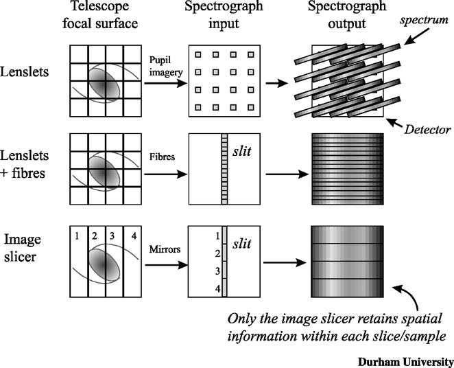
Fig. 1.— Schematic of the principle of operation of an integral field spectrograph incorporating a microlens array.
A TIGER‐type integral field spectrograph is illustrated in the top panels of Figure 1. A lenslet array is placed at the focal plane of the telescope to sample the telescope image. Each lenslet forms a small image of the telescope pupil at the entrance to a spectrograph. The light is dispersed, and a spectrum is obtained for each spatial element (lenslet) in the original telescope image.
A fiber‐lenslet–type integral field spectrograph is illustrated in the middle and bottom panels of Figure 1. In this case, each lenslet forms an image of the telescope pupil at the entrance to an optical fiber. The two‐dimensional array of optical fibers is then reformatted into a one‐dimensional slit. Light from the slit is dispersed by a spectrograph, again forming a spectrum for each spatial element in the original telescope image. In some systems a linear lenslet array is also required at the output slit to efficiently couple light from the optical fiber into the spectrograph. The system is therefore analogous to a coherent fiber bundle with microlens coupling.
The use of lenslet arrays in integral field spectrographs provides many advantages. They provide contiguous spatial sampling of the telescope focal plane with a fill factor much greater than that achievable with bare fiber bundles (typically >90% compared with 60%). Microlenses also provide an efficient way of coupling light into an optical fiber at the appropriate focal ratio for propagation in the fiber. In astronomical applications, this is usually F/4–F/6.3 They can also be used to convert the focal ratio of the telescope to one that is more suitable for use with the instrument. These gains are worthwhile only if the microlens array does not degrade the performance of the instrument.
Given the stringent specifications on modern astronomical instrumentation, it was considered necessary to characterize the performance of lenslet arrays before incorporating them into the instrument. A variety of different types of lens arrays were obtained, from various suppliers, for detailed investigation. In some cases it was found to be difficult to get detailed information from suppliers, particularly regarding image quality and encircled energy (EE) characteristics of a microlens. In general, the point‐spread function (PSF) is measured with low dynamic range over a small area (e.g., Sharp & Schmutz 1997), providing insufficient information about the quality of the lens. A series of optical tests was therefore developed to discover which types of lens array are most suitable for use in astronomy.
Although the bias of this paper is the characterization of microlens arrays for use in astronomical spectroscopy, the optical techniques described may be of considerable use for other applications.
The layout of this paper is as follows. The next section describes the microlens characteristics that need to be quantified to determine their suitability for use in an integral field spectrograph. A summary of various types of microlenses tested is given in § 3. A description of the optical test apparatus and procedures is presented in § 4. The findings of the tests are summarized in § 5. Preliminary results on the application of antireflection coatings to lenslet arrays are presented in § 6. Finally, an overall summary and conclusions are given.
2. MICROLENS REQUIREMENTS
Microlenses for use in integral field spectroscopy generally have apertures in the range 0.1–1 mm and focal ratios of F/3–F/10 and are required in arrays of up to a few thousand lenses. The lenslet array must also fulfill a number of important performance criteria: accurate lens pitch, high fill factor, consistent focal length within the array, good image quality, low surface roughness, and high absolute throughput.
Lens pitch is particularly important if the microlens array is to be used for coupling to a two‐dimensional array of optical fibers. If the position of the image formed by each lenslet does not correspond with that of the fiber core, then coupling losses will occur. The positional accuracy of fiber cores in a typical array (Murray et al. 2000) is ∼6 μm rms. Lens positioning accuracy is expected to be better than this.
High fill factors are desirable to avoid light being lost at the gaps between the lenses. A high fill factor also results in the production of less scattered light. The need for high fill factor may preclude the use of circular microlenses, which have a maximum fill factor of 90.7%. For other shapes of microlens, the lens to lens gap should be kept to a minimum.
Microlenses of spherical shape will produce images that exhibit aberrations. In integral field spectroscopy, the microlenses are illuminated on‐axis, with an off‐axis angle of typically less than 1°. The dominant aberration is therefore spherical because off‐axis aberrations such as coma and astigmatism are negligible. In practice, a microlens will have additional aberrations caused by manufacturing errors. In a TIGER‐type IFS, the image quality of the microlens determines the quality of the image at the entrance to the spectrograph. Ultimately, this will affect the spectral resolution and the number of spectra that can be accommodated on the detector without cross talk. In fiber‐lenslet–type systems, the image quality of the microlens will determine how much light is coupled into the optical fiber. Ideally, microlens image quality will be diffraction‐limited, with scattered light kept to a minimum. For larger microlenses, it may be necessary to obtain aspheric surfaces to reduce spherical aberration. All microlenses will exhibit some chromatic aberration. To reduce chromatic aberration, the microlens array can be coupled to a flint glass substrate to form an achromatic doublet. This technique works, although the substrate is plane‐parallel. As an example, consider a 1 mm aperture silica microlens, with a radius of curvature of 2.513 mm, optimized for use at 633 nm. The back focal length of the lens in silica is 8.01 mm, and the chromatic focal shift from 400 to 1000 nm is 0.16 mm. Alternatively, if a 1 mm thick silica lens is coupled to an SF6 substrate, of thickness 8.66 mm, the chromatic focal shift is reduced to 0.03 mm. This results in better images over a wider wavelength range.
In order to keep scattered light at a low level, the surface roughness of the microlens should be minimized. The presence of scattered light in astronomical spectra, usually from the adjacent microlens, will affect the accuracy of a number of spectroscopic diagnostics, such as emission‐line ratios, redshift determination, and equivalent widths.
The absolute throughput of the microlens should be as high as possible. This is the ratio of the amount of light incident at the lens surface to the amount of light that is detected at the focus of the lens within a defined aperture (often an optical fiber). Throughput will be affected by choice of lens material and the availability of antireflection coatings.
Finally, for use in infrared instruments, it is necessary that the lens array can survive being cooled to cryogenic temperature (∼77 K). This is because infrared astronomical spectrographs are operated at cryogenic temperature to reduce stray light contamination from thermal emission.
3. TYPES OF MICROLENS
In all, 16 different lenslet arrays were obtained from a variety of different manufacturers for testing and evaluation. The specification of the microlenses is summarized in Table 1. Many of these lenses have since been used in astronomical instruments, as indicated in the final column of Table 1.
 |
The lenslet arrays have been divided into groups according to the manner in which they were manufactured, and this is used to identify the lens in the first column of Table 1. The key is as follows: RIE: monolithic fused silica lenslet array manufactured by reactive ion etching; CCA: crossed cylindrical array; SR: photoresist lenslet array manufactured by surface reflow; EOG: epoxy lenses on a glass substrate; MFS: monolithic fused silica lenslet array; and PMMA: monolithic polymethylmethacrylate lenses. The lens indicated by "Conv" was produced using standard polishing techniques and can therefore be expected to have the performance of a conventional lens.
The lenses EOG and PMMA are thought to be manufactured by transferring the lens profile from a master into soft material and then curing. However, the exact manufacturing details are proprietary information and unknown. Epoxy and polymer lenses are less robust than their solid glass counterparts, and their transmission, particularly in the infrared, can be limited by the lens material.
The SR lenslet array consists of circular photoresist lenses supported on a glass substrate and was manufactured using the technique of surface reflow (Daly et al. 1990). To manufacture monolithic lens arrays, epoxy or polymer lenses can be transferred into a glass substrate by reactive ion etching. The lenslet array indicated by RIE was manufactured using this technique with the initial lens shape produced using surface reflow. There is however a limitation on the maximum sag heights that can be achieved with reactive ion etching, which prevents the manufacture of large or fast lenses. The MFS lenses were produced using a special direct chemical etching process. All lenses produced using surface reflow as part of the manufacturing process will have deviations from spherical shape caused by surface tension. Surface reflow also requires a gap between the lenses, which reduces the fill factor.
The CCA lenses are slightly unusual in that they consist of two opposing crossed cylindrical lens arrays. The two cylindrical lens arrays are cemented together, perpendicular to each other, to form an array of square lenses. They were manufactured in monolithic fused silica with broadband antireflection coatings on all surfaces. These lenslet arrays can also be obtained with aspheric surface profiles.
4. MICROLENS TESTS
To evaluate whether a particular type of microlens is suitable for use in an integral field spectrograph, a number of optical tests were devised. Of particular importance is accurate determination of image quality and EE because this provides information for direct comparison with other types of lens. Tests were also devised to determine wave front quality, pitch, and fill factor.
4.1. Measurement of PSF and Encircled Energy
As mentioned by Hutley, Daly, & Stevens (1991), there are two difficulties in the measurement of PSF and EE that need to be solved. First, a high dynamic range detector is required to measure intensity, with comparable accuracy, at both the center and boundary of the PSF. To achieve this, a Santa Barbara Instruments Group (SBIG) CCD camera was used for the tests. This is a low‐noise astronomical CCD with a dynamic range of 216. During exposures, the CCD was cooled to 0°C, thereby reducing dark current, which is the dominant source of noise. The large dynamic range of the SBIG CCD allows measurements of the PSF profile to a level of ∼10−4.5 of the peak intensity.
The second problem is to define the boundary of the area over which the total intensity is integrated. This is straightforward to achieve in software and is briefly discussed in § 4.1.2.
A diagram of the optical apparatus used to measure the PSF of a microlens is shown in Figure 2. The microlens (5) is illuminated with a collimated beam from a laser. The laser beam is first spatially filtered (1) to produce an F/4 beam and then collimated (2) to a wave front accuracy of λ/4. Helium‐neon lasers with wavelengths of 543 or 632.8 nm were used for the tests.
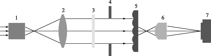
Fig. 2.— Diagram of the experimental apparatus used to measure the PSF of a microlens (not to scale). (1) spatial filter; (2) collimator lens; (3) filters; (4) diaphragm; (5) microlens array; (6) microscope objective; (7) CCD detector.
A microscope objective (6) is used to reimage the microlens PSF onto a CCD detector (7) at the appropriate magnification. Neutral density filters (3) can be placed in the laser beam to prevent saturation of the detector. A diaphragm (4) is placed just in front of the microlens under test to reduce the amount of stray light entering the system. All experiments were performed in darkness within an optical laboratory. More details regarding the experimental procedure and subsequent data analysis can be found in Lee (1998) and Ren (2000).
4.1.1. Experimental Procedure
All microlenses tested, with the exception of the CCA lenses, were plano‐convex. The lenses were illuminated with the convex surface facing the laser beam to reduce the amount of spherical aberration present in the image. The CCA lenses do not have a preferred orientation to reduce aberrations.
Initially the laser beam is adjusted to be parallel with the optical axis of the microlens. The microscope is then adjusted to bring the lens PSF into focus on the CCD. The position of maximum axial irradiance was chosen as the best focus and is readily found experimentally by observing the brightness in the core of the PSF. This is also the position that minimizes the rms wave front aberration as described in Mahajan (1991). A typical exposure sequence consisted of 20 alternate PSF and background exposures. Background exposures were taken, without the laser beam, to record the level of background illumination within the laboratory.
4.1.2. Data Analysis
The signal‐to‐noise ratio in the final image can be improved by combining many exposures. Each background exposure is subtracted from the corresponding PSF image, and the resulting images are summed to produce a final image with improved signal‐to‐noise characteristics. Subtracting the background exposures also reduces the effect of any bad pixels on the CCD.
The IRAF (Tody 1993) astronomical image analysis software package pprofile was then used to calculate the azimuthally averaged PSF and EE. Using an azimuthally averaged PSF allows the determination of intensity over many pixels at large radii, which increases accuracy. The radius of the first diffraction ring and FWHM of the azimuthally averaged PSF were measured for comparison with theoretically predicted values. Theoretical predictions of microlens performance were made using Zemax optical ray‐tracing software.
The EE is integrated within a circle of area equal to the area of the microlens. Although in principle the integration radius should approach infinity, the area of integration receives additional light from the adjacent microlenses in the array. By symmetry, this additional light is equivalent to that lost outside the area of integration. Therefore, the absolute EE can be found.
It is important in the analysis of the lens PSF to distinguish between scattered light contributed by the measurement apparatus and that due to the microlens being measured. To measure the scattered light contribution of the microscope, images were taken of a 10 μm pinhole illuminated with the laser. Diffraction by the pinhole produces a diverging beam of similar numerical aperture to that of the microlenses tested. Thus, the scattered light caused by the measurement apparatus can be expected to be similar to that produced when one measures a lens PSF. The images showed that approximately 10% of the light was scattered outside the radius of the pinhole over that expected because of diffraction (Lee 1998). The EE curve of the microlens is corrected in software to remove the effect of scattered light caused by the microscope.
4.2. Measurement of Pitch and Fill Factor
For the measurement of microlens pitch, either a ×1 microscope objective or a Nikkor 1:1 copy lens was used to simultaneously image a number of lens foci onto the CCD. The pitch can then be determined from the measured distance between the lens foci.
The image scale on the CCD was determined by imaging a calibrated reticule. The image scale was found to an accuracy of ±0.2%. The position of each lens PSF on the detector was then determined, to a positional accuracy of ±0.01 pixels, using astronomical data analysis software (PSF centroids were found using the imexamine package within IRAF). The pitch of the lenslet array, and rms error in lens position, is then found using further software (IRAF‐geomap) that calculates the best fit to the grid of lens foci.
The microscope was also used to take images of the microlens surface (e.g., Fig. 4). The fill factor of the lens array can be determined directly from these images. Features on the lens surface, such as scratches and surface roughness, can also be seen. In some cases the interlens gap was measured directly by visual inspection with the microscope.
4.3. Surface Quality
A subset of the lenses were tested to determine their surface roughness. This was achieved using a Zygo NewView 100 three‐dimensional surface structure–analyzing microscope. This instrument scans the lens surface with a white‐light interferometer to build up a three‐dimensional image. The analysis software can then be used to calculate the radius of curvature of the lens, which can be related to focal length, the surface roughness, and the surface deviation from a sphere. An example of the output from the Zygo interferometer can be seen in Figure 6.
4.4. Measurement of Wave Front
Although some information about a lens surface can be obtained using the Zygo interferometer described above, there are some limitations. The main problem is that it cannot get information about the lens shape in regions with steep curvature, e.g., the lens corners and edges. These areas are suspected to be one of the main contributors to wave front aberration and scattered light. To measure the wave front quality of the whole microlens, a modified Mach‐Zehnder interferometer was constructed. An interferometer of this type directly measures the deviation of the wave front from a perfect sphere. The optical layout of the device is shown in Figure 3. A Mach‐Zehnder interferometer was developed as an alternative to the more traditional Twyman‐Green interferometer to eliminate problems associated with stray reflections causing multiple fringe patterns (Ren 2000; Hutley et al. 1991).
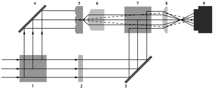
Fig. 3.— Optical diagram of the modified Mach‐Zehnder interferometer constructed to measure microlens wave front quality. (1) cube beam splitter; (2) neutral density filter; (3) plane mirror; (4) plane mirror; (5) microlens array; (6) microscope objective; (7) cube beam splitter; (8) pupil imaging lens; (9) CCD detector.
The interferometer operates as follows. Illumination is provided by a collimated beam from a helium‐neon laser with wavelength 632.8 nm. The first beam splitter (1) divides the wave front. One beam is directed via a plane mirror (4) through the microlens array (5) and brought to a focus. A microscope objective (6) recollimates the beam. The second beam is reflected by a plane mirror (3) and then combined with the first beam at the beam splitter cube (7) to generate the interferogram. A lens (8) is used to image the pupil, which is the aperture of the microlens under test, onto the CCD detector. An optional neutral density filter (2) can be used to adjust the intensity of the reference beam to maximize fringe contrast. The dotted ray path indicates how the pupil is imaged onto the CCD by lens (8).
5. SUMMARY OF RESULTS
5.1. Microlens Pitch
The pitch of a number of microlens arrays was determined using the method described in § 4.2. In all cases the pitch was found to be within 0.2% the specified value. Typical positioning errors of 3, 2, and 2 μm rms were found for the EOG, CCA, and PMMA lenses, respectively.
5.2. Fill Factor
The fill factor of a number of lens arrays was measured from images of the lens surface. An image of the surface of the RIE lenslet array, with an interlens gap of ∼12 μm, is shown in Figure 4. This can be compared with Figure 5, which shows the surface of the 0.25 mm square EOG lens array. Note that no gaps can be seen. The fill factor of the microlenses tested is summarized in Table 2.
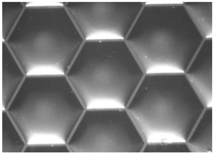
Fig. 4.— Photograph of the surface of the RIE microlens. Note the gaps between the lenses and the nonspherical appearance.
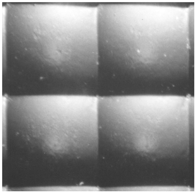
Fig. 5.— Photograph of the surface of a typical epoxy on glass microlens.
 |
In general, epoxy microlens arrays (EOG and PMMA) were found to have higher fill factors than monolithic glass lenses (RIE and MFS) and those manufactured using surface reflow (SR). A gap between the lenses is a requirement of the reflow manufacturing process. Unfortunately, the interlens gap results in an efficiency loss in an astronomical instrument, causes scattered light, and degrades the EE performance of the lens (see § 5.5). The CCA cylindrical arrays also have significant gaps between the lenses. Prieto et al. (2000) report an interlens gap of ∼30 μm for a 0.35 mm pitch lens (84% fill factor), while Sugai et al. (2000) report that the dead space between lenses is 0.15 mm for a 1.5 mm pitch lens (81% fill factor). Note that Sugai's result showed that not only was there flat land between the lenses but there was also an unusable region that deviated from the ideal lens shape.
5.3. Surface Quality
A subset of the lenses were tested to determine their surface structure using the technique described in § 4.3. The surface roughness of the lenses tested is listed in Table 2. Figure 6 shows the measured surface profile of a monolithic PMMA microlens.
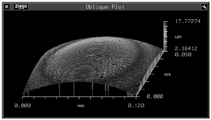
Fig. 6.— Three‐dimensional surface profile of the 0.25 mm PMMA microlens. The measured radius of curvature is 0.272 mm, and the surface roughness is 0.013 μm.
The total integrated scattered light (TIS) caused by microirregularities on an optical surface of rms surface roughness δ can be estimated from

where λ is the wavelength (Nussbaum et al. 1997). The formula is accurate for the range δ = 1–100 Å. Note that this formula does not take account of additional scattering due to particulate contamination such as dust. Table 2 also lists the predicted TIS for each microlens measured. The presence of scattered light influences the EE performance of the lens as discussed in § 5.5. Variation of TIS with wavelength was confirmed for the F/21 MFS lens at 543 and 633 nm (see Table 3), which showed degraded EE performance at shorter wavelengths.
 |
In general, replicated polymer/epoxy microlenses have higher surface roughness than monolithic microlens surfaces. This is thought to be systematic of the manufacturing process, with roughness present in the master being transferred to the lens surface. Soft epoxy lenses are also more readily damaged than glass lenses and cannot be easily cleaned to remove contamination. CCA lenses are prepared using a proprietary technique that minimizes surface roughness. Prieto et al. (2000) measured the rms surface roughness of their CCA lens array to be 0.014 μm.
5.4. Wave Front Quality
Much of the information about the wave front quality can be implied from careful analysis of the PSF. However, additional information can be obtained from an interferogram; in particular, the region of the lens that causes the wave front aberration can be determined.
Interferograms were measured with the Mach‐Zehnder interferometer for a sample of the microlens arrays. The peak‐to‐valley wave front aberration was determined by visual inspection of the interferogram. The results are listed in Table 2.
An interferogram of the 0.302 mm F/5.6 EOG microlens is shown in Figure 7. The peak to valley wave aberration is 1.5 λ at a measurement wavelength of 633 nm. The wave aberration in the central parts of the lens is small but increases rapidly toward the edges. This results in a PSF with additional light in the diffraction wings. The MFS lens also showed slight aberrations near the lens edges, but overall the wave front quality was good. This is perhaps not surprising, considering its slow focal ratio of F/21.
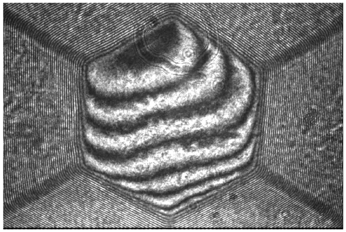
Fig. 7.— Interferogram of the 0.302 mm aperture F/5.6 EOG microlens measured at λ = 633 nm. The peak‐to‐valley wave front aberration is 1.5 λ.
Figure 8 shows the interferogram of the 0.25 mm monolithic PMMA lens. This lens has excellent performance, especially considering that it is particularly fast at F/2.2. For this lens the aberrations occur in the center of the lens rather than near the edges. This lens also has an excellent PSF and EE performance.
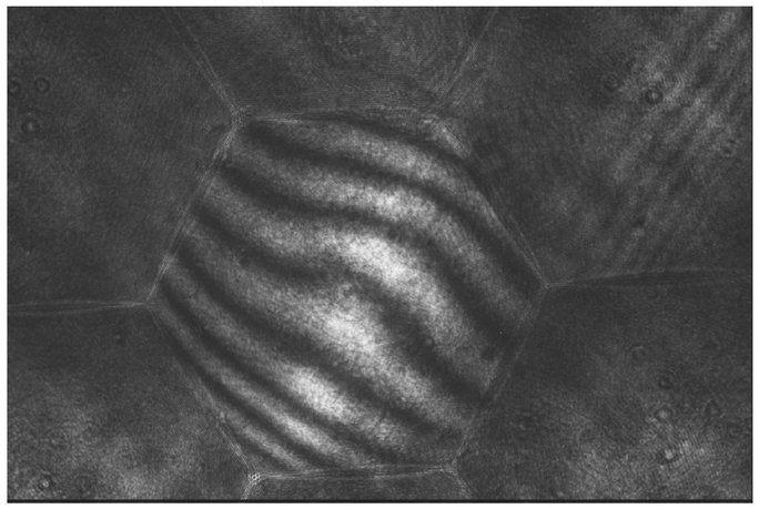
Fig. 8.— Interferogram of the 0.25 mm aperture PMMA microlens measured at λ = 633 nm. The peak‐to‐valley wave front aberration is 0.5 λ.
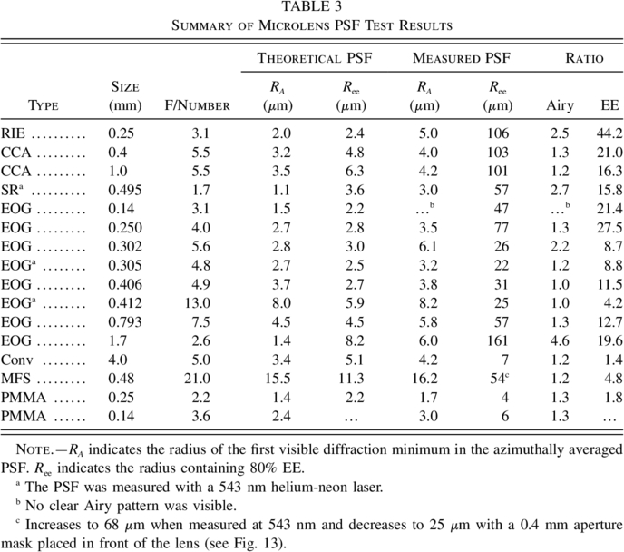
5.5. Image Quality and Encircled Energy
All microlenses listed in Table 1 were tested to determine their PSF and EE characteristics, and the results are summarized in Table 3. Theoretically predicted values of radius of first diffraction minimum, and radius containing 80% EE, are also given for comparison with the measured values. Theoretical predictions were performed using Zemax optical ray‐tracing software.
All lenses tested have a PSF that shows diffraction minima except the rectangular 0.14 × 0.2 mm EOG lens, which had an aberrated PSF without clear minima. Figures 9 and 10 show examples of PSF images for a selection of the lenses tested. For some lenses the first observable diffraction minima occur at a larger radius than predicted, indicating the presence of significant aberrations that make the Airy ring unobservable. This is noticeable for lenses manufactured with surface reflow (RIE and SR). The cause of aberrations with reflow lenses is surface tension at the lens edge distorting the lens profile (Daly et al. 1990). Note that broadening of the microlens PSF by the measurement apparatus is negligible.
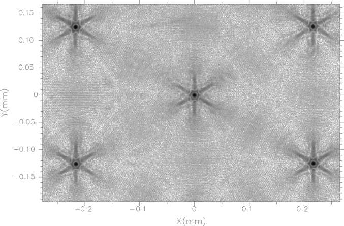
Fig. 9.— Image of the RIE lens PSF measured at λ = 633 nm. The image is shown with a logarithmic intensity scale. The diffraction pattern of a hexagonal lens can be clearly seen, although the first Airy ring is not visible because of the presence of aberrations.
Fig. 10.— Image of the 0.4 mm CCA lens PSF taken at λ = 633 nm. The image is shown with a logarithmic intensity scale.
An image of the PSF produced by the RIE microlens can be seen in Figure 9. The measured radius of the first minima in the PSF is ∼5.0 μm; however, the predicted value is 2.0 μm, indicating the presence of significant aberrations in the lens. The image also shows the presence of a large amount of scattered light between the microlens PSFs. The scattered light level is ∼10−3 of the peak intensity (see Fig. 11) and results in poor EE performance (see Fig. 12).
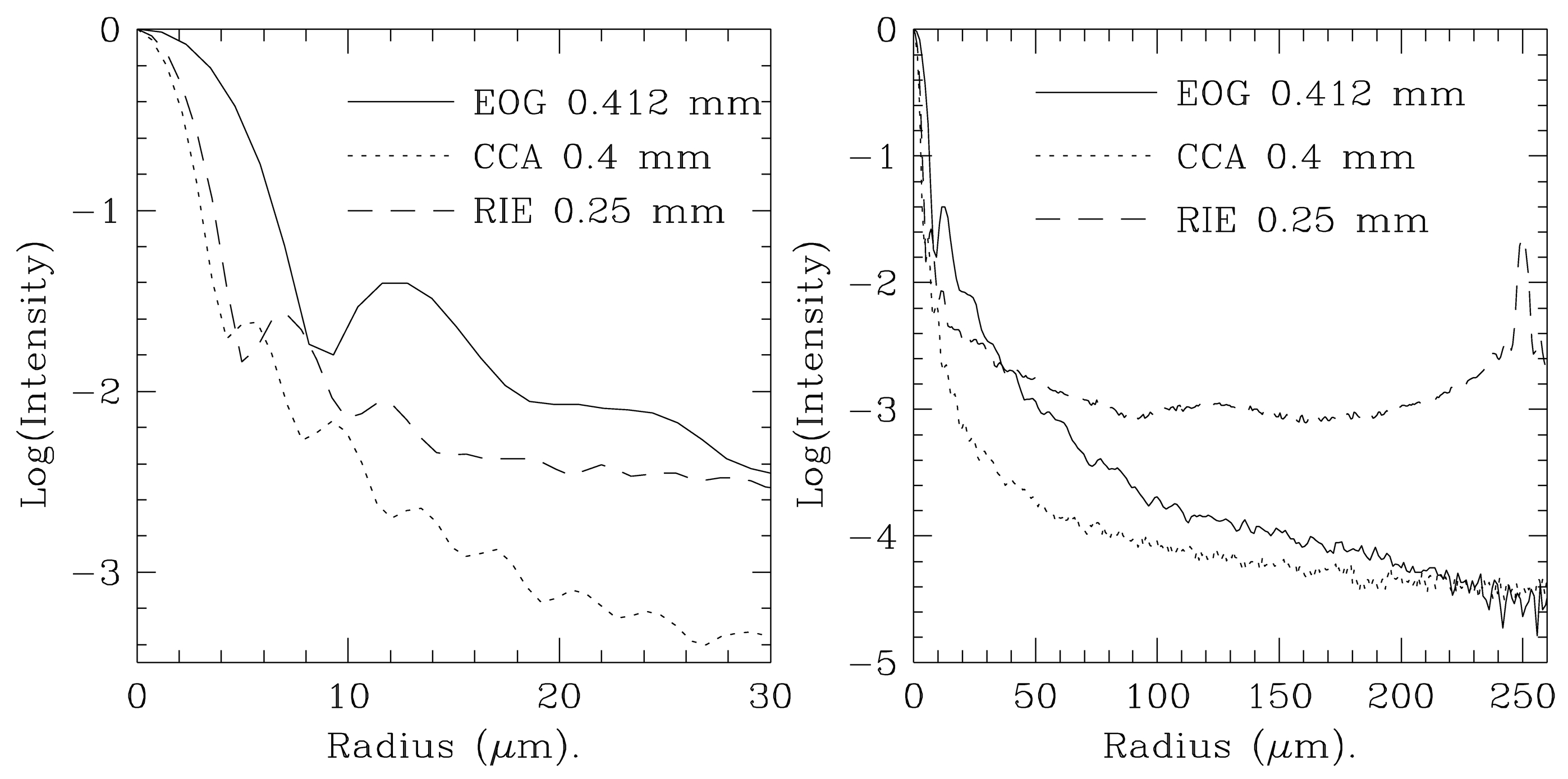
Fig. 11.— Azimuthally averaged PSF profile of the 0.412 mm F/13 EOG lens, 0.25 mm F/3.1 RIE lens, and 0.4 mm F/5.5 CCA lens. The plots have been normalized so that the peak intensity equals 1. The PSF of the EOG lens is close to diffraction‐limited. Note the large amount of scattered light present with the RIE lens.
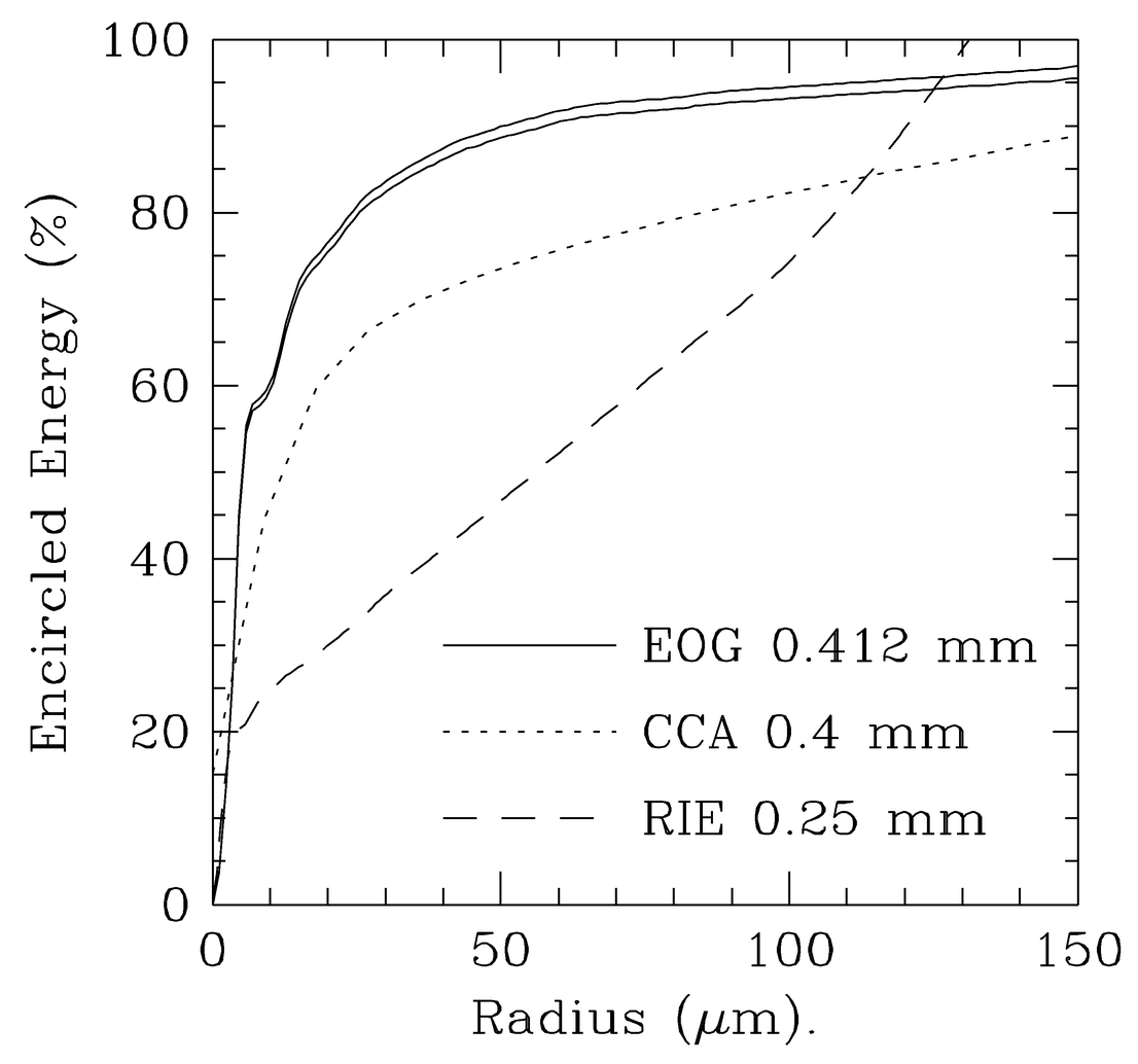
Fig. 12.— EE vs. radius for the 0.412 mm F/13 EOG lens, 0.25 mm F/3.1 RIE lens, and 0.4 mm F/5.5 CCA lens. The experimental error in EE is represented by the two lines (upper and lower limits) plotted for the EOG lens.
The PSF produced by the 0.4 mm CCA lens can be seen in Figure 10. The diffraction pattern caused by a square aperture can be clearly seen. The first diffraction minimum occurs at 3.9 μm, compared with the theoretical prediction of 3.5 μm, indicating close to diffraction‐limited images. The prominent stripes that appear in this image are the single‐slit diffraction patterns caused by the 25 μm gap between the cylindrical lenses.
Plots of the azimuthally averaged PSF for a selection of the lenses tested are shown in Figure 11. Note the low‐intensity background of scattered light, which is present even at large radii. Figure 12 shows the corresponding plot of EE versus radius. Note that the EE curves are normalized such that 100% EE is contained within the area of the lens (they are not normalized by the fill factor).
To accurately determine the effect of the lens edges and interlens gaps on EE performance, the MFS lens was tested with and without a 0.4 mm pinhole mask in front of the lens. The resulting data, shown in Figure 13, show a 20% increase in EE when the lens edges are masked. This indicates that the lens edges (and associated aberrations) and interlens gaps contribute significantly to the amount of scattered light.
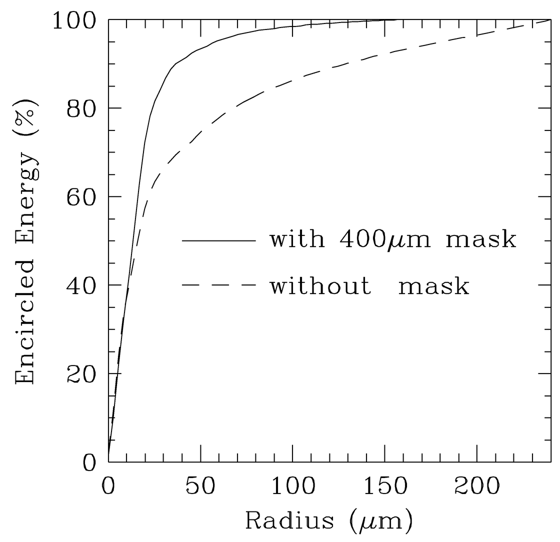
Fig. 13.— EE vs. radius for the 0.48 mm MFS microlens. The measurement wavelength was 543 nm.
5.6. Analysis of PSF Results
A measure of the relative image quality of a microlens can be obtained by comparing the measured performance with the theoretically predicted performance. This is done in the final two columns of Table 3, which list the ratio of measured Airy radius to predicted Airy radius and ratio of measured radius containing 80% EE to predicted radius, respectively. For a perfect lens, this ratio will be unity.
The conventional 4 mm lens gives the best performance. The best microlens overall is the 0.25 mm monolithic PMMA lens, which has a high‐quality PSF and excellent EE performance. The F/21 monolithic fused silica and F/13 epoxy on glass lenses also have good performance, although this is perhaps not surprising given their relatively slow focal ratios. The EE performance of the EOG lenses is limited mainly by surface roughness causing significant scattered light. For the RIE, CCA, and SR lenses the EE performance is reduced by the significant interlens gaps causing light losses. The CCA lenses do however have good image quality.
5.7. Cryogenic Testing
A number of lens arrays were cooled to cryogenic temperature (77 K) to test whether or not they would survive being thermally cycled. Both the EOG and RIE lenses showed no visible deterioration after a number of cycles. Tests with the CCA lens were less successful as the epoxy bond between the crossed cylindrical lenses failed at low temperatures, causing the lenses to separate.
6. ANTIREFLECTION COATINGS
Efficiency gains can be made if it is possible to use antireflection coatings on the surface of the microlens. Monolithic silica lenses can be coated in the conventional manner using thermal evaporation vacuum coatings. However, polymer or epoxy lenses cannot be coated in this manner because the heat involved will damage the fragile lens surface.
The use of ion‐assisted deposition (IAD) coatings offers one solution. This process does not require the lens to be heated and can therefore be applied to sensitive lens materials. Initial trials were performed on the 0.302 mm F/5.6 EOG lens. Unfortunately, the coating was not successful as the lens surface roughness was found to have increased to 0.13 μm rms after coating. The radius of curvature was also found to have been changed by the coating process. Transmission measurements, performed on part of the substrate that did not contain lenses, showed a decrease in the transmission of the lens after coating.
IAD coating was also trialed at Stiltint Industries Limited (UK) on the 0.406 mm F/4.9 EOG lens. This was much more successful, with a 3% gain in transmission measured after coating. A small change was measured in the EE performance after coating, with the 90% EE radius increasing from 54 to 71 μm but with improvements at radii less than 30 μm.
7. CONCLUSIONS
This paper began with a description of the use of lenslet arrays in modern astronomical spectrographs. This imposes demanding requirements on the lens performance; in particular, good image quality and high fill factors are necessary. A number of lenslet arrays were tested to determine their suitability for use. To achieve this, a series of optical tests were developed to measure lens PSF, EE, surface quality, and wave front quality. The experimental apparatus used to perform these tests was described in detail.
All lenslet arrays tested were found to have accurate pitch. Fill factors were measured and found to be between 88%, for surface reflow lenses, and 99%, for epoxy lenses. The surface quality was generally found to be better for monolithic glass lenses than replica epoxy lenses. Wave front quality measurements showed that the area near lens edges can cause aberrations. Most lenses had a PSF with a clearly observable diffraction pattern indicating the presence of only minor aberrations. The EE performance was found to be degraded by the presence of scattered light caused by surface roughness or interlens gaps. The monolithic PMMA lens, monolithic fused silica lens, and epoxy on glass lens were found to give the best overall performance. Of course, the final choice of lens may not simply be dictated by performance but by cost and ability to manufacture to the correct specification without limitations imposed by manufacturing techniques.
A number of the lenslet arrays tested were considered of sufficient quality to be used in various astronomical spectrographs. The SPIRAL spectrograph at the Anglo‐Australian Telescope (Lee & Taylor 2000) uses an F/5.5 CCA microlens array to couple light from the telescope into a fiber bundle. A CCA lens array was chosen in this case because of the need for a relatively large pitch (1 mm). The CCA lenses have aspheric surfaces, which allows good image quality to be obtained even with a lens of this size. Image quality is very important in this application to achieve high coupling efficiency between the telescope and the optical fibers. A similar array containing 6400 CCA lenses has also been successfully used in the European Southern Observatories VIMOS instrument (Prieto et al. 2000). Monolithic fused silica lenses have been used in the Potsdam multiaperture spectrograph and indicate excellent performance (Roth et al. 2000). The SMIRFS‐IFU instrument (Haynes et al. 1999) uses an F/13 hexagonal epoxy on glass lenslet array at the input to a fiber bundle and square F/7.5 EOG lenses at the output of the fiber bundle. The TEIFU instrument (Murray et al. 2000) also uses an epoxy on glass lenslet array.
The authors would like to thank the numerous staff at the various companies that supplied microlens arrays, especially Marty Levine and Carol Dwyer from Adaptive Optics Associates, Tom Harvey from Epigem Ltd., and Dirk Hauschild from Lissotschenko Mikrooptik GmbH. We thank Graham Murray for organizing the IAD coatings. We also thank Robert Content, Colin Dunlop, John Webster, George Dodsworth, and Keith Taylor. Finally, we acknowledge the work of David Nicolas in obtaining some of the PSF data.
Footnotes
- 3
This focal ratio is chosen to minimize focal ratio degradation. This effect causes light entering a fiber at a given focal ratio to exit at a faster focal ratio (Carrasco & Parry 1994).