


Abstract
A technology of arrays of distributed-feedback semiconductor lasers for the spectral region of 1.55 μm and their characteristics are presented. Stable single-frequency lasing with a side mode suppression ratio higher than 25 dB is demonstrated. The possibility of continuous wavelength tuning in a range of up to 7 nm is shown.
Export citation and abstract BibTeX RIS
1. Introduction
Sources of single-frequency radiation based on 1.55 μm semiconductor lasers are critically important components of fibre-optic communication lines. The most compact and reliable light sources with extremely narrow emission lines are distributed feedback (DFB) semiconductor lasers [1, 2]. Experimental studies and development of these lasers began as long ago as the 70 – 80s of the last century [3, 4]. Further development of the technology of DFB lasers led to the creation of lasers with very high coupling coefficients [5, 6], which allowed one to obtain very stable single-frequency operation and increase the yield of these lasers. At present, permanent interest in this type of semiconductor lasers is related to a new concept of versatility of components in telecommunication networks [7], which suggests the application of tunable single-frequency lasers as transducers. Apart from the technology of DFB lasers, there exist several alternative directions of development of tunable single-frequency semiconductor lasers, in particular, the use of short external cavities [8, 9] and controllable distributed Bragg reflectors [10]. The wavelength of a DFB laser can be tuned mainly by changing the temperature of its active region. It is well known that the rate of temperature tuning of laser wavelength in the spectral region of 1.55 μm is ∼ 0.1 nm K−1, which restricts the spectral tuning range by a value of 2 – 3 nm because fast heating leads to a close roll-over of the light – current characteristic and a decrease in the output power [11]. In this connection, the most promising approach to obtaining tunable single-frequency sources of radiation in the region of 1.55 μm is the fabrication of DFB laser arrays with individual periods of distributed feedback gratings for each emitter. Ongoing extensive studies of these lasers show that this approach is promising for creating single-frequency tunable lasers emitting in the aforementioned region [12 – 14].
2. Experimental samples
To produce linear arrays of DFB lasers, we chose two-stage epitaxy, i.e., the epitaxial growth of the heterostructure was interrupted after growing the waveguide layer and then DFB diffraction gratings were formed on this layer with subsequent epitaxial regrowth. The heterostructures for the DFB laser arrays were grown at the Connector Optics LLC on a Riber 49 molecular beam epitaxy (MBE) reactor. The same equipment was used to regrow the semiconductor wafers with formed diffraction gratings for DFB laser arrays.
As was shown previously [15], to achieve high stability of single-frequency lasing with temperature tuning of the DFB laser spectrum, it is necessary to form a grating near the active region (to provide a high coupling coefficient). As a result, the optical losses introduced in the case of fabrication of DFB lasers by the regrowth technique may considerably exceed the optical losses in the case of formation of gratings on the surface of the upper waveguide cladding, because of which it is necessary to use active regions with high gains. Double heterostructures with a bulk layer based on quaternary solid solutions InGaAsP demonstrate a high gain, which explains the choice of these materials for developing the technology of regrowth of diffraction gratings by molecular-beam epitaxy and for fabricating 1.55 μm single-frequency semiconductor DFB laser arrays. The detailed description of the structure is given in [15].
After the first stage of the epitaxial growth of heterostructures, diffraction gratings with periods of 468.6, 468, 467.4, and 466.8 nm were formed on these structures by electron-beam lithography at the JSC OKB-Planeta using a Raith Voyager system. This system is intended for formation of images in an electron resist film with a minimum (to 10 nm) topological element size. The lithograph contains a system for electrostatic electron-beam deflection in combination with a pattern generator operating at 50 MHz, which makes it possible to achieve a processing rate of up to 1 cm2 h−1 (at 50 % filling of the exposure region). The exposure field size amounts to 500 μm with dynamic correction of parameters in a real-time mode. The system does not require stitching of write fields, which is important for fabricating long elements, such as optical fibres and repeating structures like photonic crystals, including DFB diffraction gratings. This system can be used not only as a lithograph but also as an electron microscope with a maximum magnification up to 100000×. In addition, it is possible to perform measurements at different angles to the studied sample surface.
To determine the optimum exposure dose in order to form high-quality masks in the electron resist for subsequent formation of DFB gratings, we fabricated the masks at exposure doses of 75, 80, and 85 μC cm−1 (Fig. 1). As is seen from Fig. 1, the optimum exposure dose for obtaining a high-quality mask in an electron resist for fabricating DFB gratings is 85 μC cm−1.
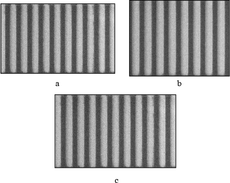
Figure 1. SEM images of DFB laser arrays at exposure doses of (a) 75, (b) 80, and (c) 85 μC cm−1.
Download figure:
Standard imageTo form a periodic structure and DFB in the waveguide region of the laser, which consists of quaternary solid solutions InGaAsP 120 nm thick, it is necessary to obtain a mesa structure ∼80 nm deep. Our experiments show that the most efficient method for obtaining high-quality DFB grating is plasma-chemical etching.
The etching was performed in inductively coupled plasma using a Sentech SI500 plasma etcher. However, to achieve high-quality etching, i.e., without strong inclination of the side walls of the grating grooves and a developed morphology of the bottom, it was necessary to heat the samples, which led to degradation of the electron resist mask. Because of this, we had to select a so-called hard mask. It was experimentally found that a two-layer hard mask consisting of a SiO2 layer 50 nm thick and a 30-nm Al layer allows obtaining high-quality diffraction gratings. The aluminium layer served as a mask for etching SiO2. The topological mask in the Al layer for etching SiO2 was formed by lift-off lithography. As a mask for lift-off lithography, we used a two-layer resist consisting of LOR 1A resist and PMMA 600K positive electron resist. The topological mask formed in Al by this method is shown in Fig. 2a.
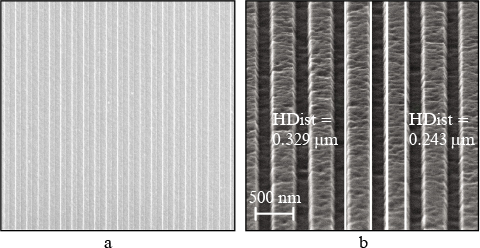
Figure 2. SEM images of (a) Al-based masking coating and (b) DFB array made using plasma-chemical etching.
Download figure:
Standard imageFigure 2b shows a photograph of the DFB diffraction grating formed in the In0.72Ga0.28As0.6P0.4 waveguide layer by plasma-chemical etching in inductively coupled plasma through the hard combined mask based on SiO2/Al. The described method allows formation of high-quality DFB diffraction gratings with a relief depth of ∼80 nm. As was shown in [15], such a large etching depth makes it possible to achieve a coupling coefficient of about 400, which, in turn, ensures a high stability of single-frequency lasing with temperature tuning of the emission spectrum. As a result, we formed DFB diffraction gratings with four different periods. The transverse size of the grating region was 50 μm, while the distance between neighbouring gratings was 200 μm. Thus, the fill factor was 20 %, which allowed us to considerably decrease the time of electron-beam lithography. The regions with gratings were alternated so as to form arrays of four emitters with different wavelengths.
The next step in the fabrication of the experimental samples of DFB laser arrays was the epitaxial regrowth of the semiconductor wafers with etched diffraction gratings. The emitter and contact layers were grown on the laser structures. The layers are described in [15].
The final step in the fabrication of DFB lasers was the formation of ridges followed by dividing the wafers into individual chips and soldering the chips on primary heat sinks. Since the diffraction gratings were formed with different steps, at the grating formation stage we imbedded alignment marks, which made it possible to form 5 μm wide ridges on the regrown layers over the diffraction gratings by lithography and wet etching. The ridges were formed by etching shallow mesa-grooves in the heterostructure. Figure 3a shows a groove formed in the heterostructure of a DFB laser. Then, the structure was covered by a SiO2 dielectric layer, and windows on the top of the ridges were opened to form the upper contact. Figure 3b shows a mesa-groove with deposited dielectric. The photograph was made before opening the windows for the upper contact.
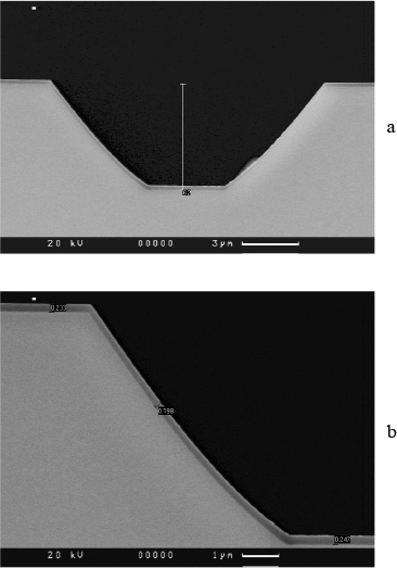
Figure 3. SEM images of (a) mesa-grooves formed on the heterostructure of DFB lasers by wet etching and (b) mesa-groove with deposited dielectric.
Download figure:
Standard imageAfter formation of the ridges, the structure was divided into individual laser chips 0.5 mm long, which contained four emitters each. The chips were then soldered on the primary heat sink. A photograph of the DFB laser array with four emitters on the heat sink is given in Fig. 4. The chips were soldered with a common contact formed from the substrate side. This design hinders heat removal from the laser but, instead, allows individual control of each laser of the array.
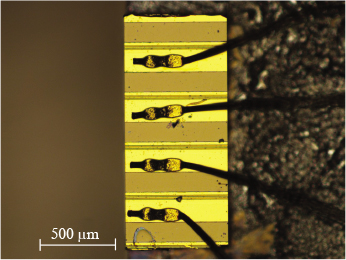
Figure 4. Photograph of a chip of a DFB laser array consisting of four emitters on a primary heat sink.
Download figure:
Standard image3. Experiment
The fabricated samples of DFB laser arrays were studied in a pulsed mode. The pump current pulse duration was 90 ns, and the pulse repetition rate was 48 kHz. The studied samples were mounted on a copper heat sink, the temperature of which was stabilised using a thermoelectric cooler.
The measurements of the light – current characteristics show that the threshold currents of individual emitters at room temperature lie within the range 500 – 700 mA, and their output powers exceed 100 μW. The low output powers of the lasers are explained by strong heating of the heterostructure due to high threshold currents. The power was measured by a calibrated Newport 841PE power meter with a Newport 818-IR germanium photodetector. A typical light – current characteristic of the DFB laser array at a temperature of 288 K is presented in Fig. 5.
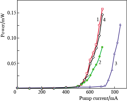
Figure 5. Typical light – current characteristic of a DFB laser array at room temperature; 1 – 4 are the laser numbers in the chip.
Download figure:
Standard imageThe spectral characteristics were measured on an MDR-23 monochromator with a 600-line mm−1 diffraction grating. An Fd-7G germanium photodiode was used as a photodetector. To decrease the effect of parasitic illumination on the measurement quality, we used the lock-in detection technique. The input/output slit size was 0.1 mm, which provided a spectral resolution of 0.26 nm. The choice of the monochromator slit sizes was based on the following requirements: first, the resolution should be better than the intermode distance of a 0.5-mm Fabry – Perot resonator (formed by the cleaved faces of the chip) and, second, the signal-to-noise ratio should be high, which, in turn, provides the possibility of measuring high side-mode suppression ratios (SMSRs). The study of the spectral characteristics revealed stable room-temperature single-frequency lasing for all emitters of the array. The SMSR exceeded 25 dB.
A typical emission spectrum of an array consisting of four DFB lasers is given in Fig. 6. The total spectrum covered by this array (i.e., the spectral distance between the outermost lines of individual emitters at one and the same temperature) was ∼5.5 nm, which is close to the calculated value of 6 nm. The deviation of the spectral distance between the lines with the shortest and longest wavelengths from the calculated value is obviously explained by a slight deviation of the effective refractive index used in calculation from the real value. The measured spectral parameters show that the experimental samples of DFB laser arrays can be used as sources of tunable single-frequency radiation in the region of 1.55 μm.
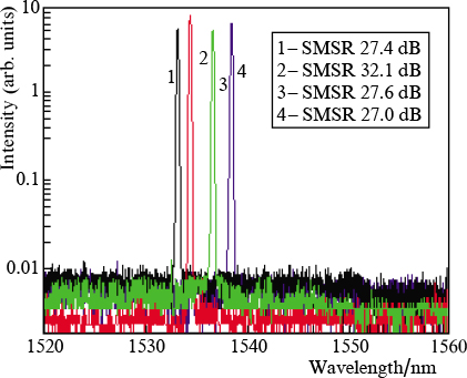
Figure 6. Typical emission spectrum of a DFB laser array at room temperature.
Download figure:
Standard imageThe temperature tuning of the DFB laser array was studied in the range 288 – 308 K (15 – 35 °C). Figure 7 shows the spectral tuning of each emitter of the DFB laser array by temperature. One can clearly see that the independent control of each emitter of the array makes it possible to achieve continuous wavelength tuning within a range of 7 nm. Our study showed high (exceeding 25 dB) SMSRs for each of the emitters in the entire temperature range. The temperature dependence of SMSRs for each emitter of the array is shown in Fig. 8.
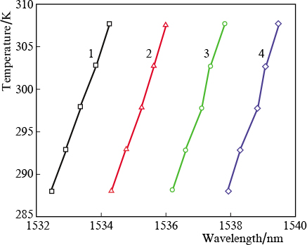
Figure 7. Dependence of the emission wavelength on temperature for each emitter of the DFB laser array.
Download figure:
Standard image
Figure 8. Temperature dependence of side-mode suppression ratio for each emitter of the DFB laser array.
Download figure:
Standard imageIt should be noted that the developed technology can be successfully used for fabricating high-power single-frequency broad-aperture DFB laser arrays with curved-groove diffraction gratings [16, 17].
4. Conclusions
Thus, we presented a technology of DFB laser arrays for the spectral region of 1.55 μm. The fabricated samples of DFB laser arrays demonstrate stable single-frequency lasing with SMSRs exceeding 25 dB. The performed study of the spectral characteristics in the temperature range 288 – 308 K shows the possibility of continuous tuning within a spectral range of 7 nm with a high (exceeding 25 dB) SMSR, which means that the developed technology can be used for fabricating sources of tunable single-frequency laser radiation in the spectral region of 1.55 μm. The high threshold currents obtained in the course of experiment are explained by the use of the active region based on a double heterostructure, which is characterised, apart from a high modal gain, by a high transparency current and, hence, a high threshold current. The tunable sources of single-frequency laser radiation in the region of 1.55 μm based on the proposed molecular-beam epitaxy regrowth and fabrication of DFB laser arrays can be developed in the future with the use of quantum-well active regions [18, 19], which ensure high gains, lower threshold current densities, and, as a result, weaker heating of chips than in the case of bulk active regions.