


We study numerically absorption optical spectra of n-doped InAs/In015Ga085As/GaAs quantum dot-in-a-well systems. The absorption spectra are mainly determined by the size of a quantum dot and have weak dependence on the thickness of quantum well and position of the dot in a well. The dot-in-a-well system is sensitive to both in-plane and out-of-plane polarizations of the incident light with much stronger absorption intensities for the in-plane-polarized light. The absorption spectrum of in-plane-polarized light has also a multi-peak structure with two or three peaks of comparable intensities, while the absorption spectrum of out-of-plane polarized light has a single well-pronounced peak.
I. INTRODUCTION
Infrared photodetectors were the subject of intensive experimental and theoretical research for the last few decades.1 Such photodetectors are based on either intrinsic free carrier or impurity absorptions of an incident light or intersubband photo-absorption in low-dimensional systems, such as quantum wells or quantum dots. One of the main goals of infrared photodetectors is to achieve desirable high temperature photoresponse at controllable frequency. Recently, highly p-doped GaAs/AlxGa1-xAs semiconductor photodetectors, operating at high temperature in the wavelength range of 3-5 μm, were reported.2,3 The photoresponse of such photodetector is due to optical transitions between the heavy (light) hole and split-off subbands.2,3 The photoresponse of split-off photodetector can be controlled by variation of composition of the material of the photodetector and by the strength of its doping, although the frequency range of its photoresponse is still relatively broad. One way to make the photoresponse of the photodetector narrow is to reduce the dimensionality of the system, i,e, to introduce additional dimensional quantization, which is realized, for example, in the quantum well4 and quantum dot5 photodetectors.
Due to effective zero dimensionality of the quantum dots, quantum dot photodetectors have some advantage over quantum well photodetectors.5 For example, quantum dot photodetectors are sensitive to both x- and z-polarizations of the incident light, while quantum well photodetectors are sensitive to z-polarization only. Here z-direction is the growth direction. Therefore the unique feature of the quantum dot photodetectors is that they are sensitive to the normally incident light. The infrared photodetectors based on the quantum dots or combination of the quantum dots and quantum wells were realized experimentally.6–9
Semiconductor quantum dots or “artificial atoms” are zero dimensional systems, the electron dynamics10 in which are confined in all three spatial directions. Such systems have properties between those of bulk semiconductors and discrete molecules.11 Due to unique transport and optical properties of quantum dots, they have found their applications in transistors,12 solar cells, light emitting diodes,13 photodetectors,6–9 diode lasers,14 medical imaging,15 and quantum computing.16
There are two different approaches how the trapping potential of semiconductor quantum dot can be realized. In the first approach the trapping potential is produced by confining electrostatic gate potentials. Such quantum dots usually have large size (∼100 nm) with large number of electrons and show unique transport properties,17 such as Kondo effect18 and Coulomb blockade.17 In the second approach a quantum dot is realized as a small enclosure of one semiconductor material in another material.19 In this case the trapping potential is introduced by conduction or valence band offsets of the corresponding materials. Such quantum dots can have small size (∼10 nm) and can be grown by Stranski-Krastanow technique. These quantum dots can be used as an active element in infrared quantum dot photodetectors. Due to discrete energy spectrum of the quantum dots, they support not only the frequency tunability but also the high-temperature operation of the photodetectors. Such high-temperature (240–300 K) operation of a tunneling quantum-dot infrared photodetector has been demonstrated experimentally in Ref. 9.
Additional control of the optical properties of quantum dots can be realized by placing quantum dots inside a quantum well. Such dot-in-a-well (DWELL) structures have two main types of optical transitions: (i) between the states of the quantum dot and (ii) between the states of the quantum dot and the states of the quantum well. Using femtosecond spectroscopy, long carrier lifetimes have been reported20 in DWELL heterostructures and it was also demonstrated that these structures are bias-tunable and are able to operate in the mid infrared (MIR, 3-5 μm), long infrared (LIR, 8-12 μm) and very long infrared (VLIR, > 14 μm) regimes with the peak of the spectral response gradually red shifting as the thickness of the InGaAs layer is increased from 10 Å to 60 Å. Seller et al.21 has demonstrated the optimized growth of DWELL QD devices for 1.3 μm lasers in which far-IR modulation technique was applied to determine the electron and hole quantization energies of QDs. It was reported that electron and hole quantization energies of 46.7 ± 0.2 and 13 ± 1 meV, respectively were obtained for the DWELL QD device.
A typical two color photoresponse was reported22 for InAs/InGaAs DWELL detector at 130 meV – 160 meV (9 μm – 7 μm) and at 230 meV (5 μm) and the possibility of tuning of the spectral range by varying the QW thickness was observed. The demonstration of a two-color infrared focal plane array based on a voltage-tunable quantum DWELL design was reported.23 The active region of the structure consisted of multiple layers of InAs quantum dots in In0.15Ga0.85As quantum well. It was shown that spectral response has a peak at 5.5 mm for lower biases and at 8–10 mm for higher biases. Three-color InAs–InGaAs quantum DWELL detectors, which have different sizes of quantum wells and quantum dots, were reported in Ref. 24. The photoresponse of such DWELL detector was at three distinct wavelengths: 6.25 μm, 10.5 μm and 23.3 μm. The first two peaks correspond to the bound to bound transitions between the ground state in the dot and the states in the well, while the long wavelength response corresponds to optical transitions between the states of the dot.
In Ref. 25 the effect of doping on the dark current of InAs/In0.15Ga0.85As DWELL photodetectors was studied. It was shown that the dark current increases monotonically with increasing the doping levels. The optimal doping for such photodetectors corresponds to 1 electron per quantum dot. Enhancement of the optical sensitivity of DWELL photodetector to the s-polarized light compared to QD photodetectors was also reported in Ref. 26.
In the present paper we study n3-doped DWELL photodetectors,22,23 addressing the problem of tunability of the photoresponse frequency of such photodetectors. Namely, we study numerically the intraband optical absorptions within the conduction band of InAs/InxGa1-xAs/GaAs DWELL structures. We study how the size of the dot, the size of the quantum well, and the position of the dot within the well affect both the frequency and the intensity of the optical transitions. The quantum dots under investigation can be realized experimentally by Stranski-Krastanow growth technique, which can provide relatively high control over the size of the dot. The electronic states and optical transitions in DWELL system were found numerically within the effective mass model by employing the Nextnano27 software package. We have found numerically the absorption spectra for both z and x polarized light, where z-direction is the growth direction. The size of the base of QD has been varied from 5 nm to 15 nm and the thickness of QW has been varied from 6 nm to 15 nm. In all calculations below we assume that the In content is x = 0.15 and the doping of the DWELL photodetector corresponds to 1 electron per quantum dot.
II. MODEL AND MAIN EQUATIONS
We consider an isolated semiconductor quantum dot placed in a quantum well. The type of the structure is InAs (quantum dot)/InxGa1-xAs (quantum well)/GaAs (substrate). We assume that the quantum dot has a pyramidal shape with a square base. The four sides of the pyramidal quantum dot are oriented in the (011), (0-11), (101) and (-101) directions, respectively. Such quantum dot is characterized by two geometric parameters: the length, b, of the side of the square base of the dot; and the height, h of the dot. In all calculations below we fixed the ratio h/b assuming that h = b/3. Under this condition, the size of the quantum dot is determined by only one parameter, e.g. by the length b, which is defined below as the size of the quantum dot. In our calculations, we vary both the size of the quantum dot and the thickness of the quantum well. The thickness of the substrate above and below the quantum well is 15 nm in all three directions, x, y, and z. The shape and the position of the quantum dot and the orientation of the quantum dot in the quantum well and substrate layer are shown schematically in Fig. 1. To study the dependence of the photoresponse on the position of the quantum dot in the quantum well, we consider two possible placement of the quantum dot: one at the top of the quantum well [Fig. 1(a)] and another one at the bottom of the quantum well [Fig. 1(b)]. In all calculations below we assumed that the In content is 0.15, i.e., we consider InAs/In0.15Ga0.85As/GaAs DWELL system.

Schematic illustration of the dot-in-a-well system. The quantum dot (InAs) is at the top (a) and at the bottom (b) of the quantum well (In0.15Ga0.85As).
Schematic illustration of the dot-in-a-well system. The quantum dot (InAs) is at the top (a) and at the bottom (b) of the quantum well (In0.15Ga0.85As).
To find the energy spectrum and the corresponding wave functions of the DWELL system we employ the one band (conduction band) effective mass model. This model is described by the following Hamiltonian
Where |$\vec p = - i \hbar \frac{\delta }{{\delta \vec r}}$| is the operator of 3D momentum, |$m^{\ast} ({\vec r})$| is the conduction band effective mass, and |$V({\vec r})$| is the conduction band offset energy, which should be considered as an effective potential. Both the effective mass |$m^{\ast} ({\vec r})$| and the conduction band offset |$V({\vec r})$| are the step-like functions, which take three different values, corresponding to three different materials of the DWELL system: quantum dot, quantum well, and substrate. Within the effective mass model we solve the corresponding Schrödinger equation numerically by using the Nextnano software package.27 This package calculates the energy spectrum, transport and optical properties of semiconductor nanostructures. The geometric parameters of the quantum dot and the quantum well, used in simulations of the DWELL system, are shown in the Tables I and II, where the sizes of the system, geometric orientation of the quantum dot, and the parameters of the model are listed.
Dimensions of the quantum well and the pyramidal quantum dot, which are used in our calculations. The dot base is a square and we define the dot size as the length, b, of the side of the square. The dot height is 1/3 of the dot size, h = b/3.
| QD size, b (nm) | QD height, h (nm) | QW thickness (nm) | Position of the Dot inside the QW |
|---|---|---|---|
| 5 | 1.67 | 6, 10, 14 and 18 | Top / Bottom |
| 9 | 3 | 6, 10, 14 and 18 | Top / Bottom |
| 12 | 4 | 6, 10, 14 and 18 | Top / Bottom |
| 15 | 5 | 6, 10, 14 and 18 | Top / Bottom |
| QD size, b (nm) | QD height, h (nm) | QW thickness (nm) | Position of the Dot inside the QW |
|---|---|---|---|
| 5 | 1.67 | 6, 10, 14 and 18 | Top / Bottom |
| 9 | 3 | 6, 10, 14 and 18 | Top / Bottom |
| 12 | 4 | 6, 10, 14 and 18 | Top / Bottom |
| 15 | 5 | 6, 10, 14 and 18 | Top / Bottom |
Parameters of the numerical model of DWELL system.
| Quantum Dot | InAs |
| Quantum Well | In0.15Ga0.85As |
| Substrate | GaAs |
| Pyramidal Quantum Dot sides | {011} |
| Temperature | 4K |
| #Electronic States | 20 |
| Model | Effective Mass Method |
| Indium Content | 0.15 |
| 40Conduction band mass In0.15Ga0.85As | 0.05968975 |
| 40Conduction band mass InAs | 0.026 |
| 40Conduction band mass GaAs | 0.067 |
| 27Conduction band edge In0.15Ga0.85As (eV) | 1.30 eV |
| 27Conduction band edge InAs (eV) | 0.52 eV |
| 27Conduction band edge GaAs (eV) | 1.50 eV |
To find the intraband optical transitions within the conduction band of the DWELL system, we calculate 20 eigenstates of the system and then find the optical matrix elements between these states. The optical transitions (absorption) in such system are allowed only at a finite n-doping of the quantum dot system. Such n-doping introduces a finite number of electrons into the quantum dot. We assume that the electron concentration is low enough, so that each quantum dot is occupied by one electron only. In this case we do no need to take into account the inter-electron interactions, and at low temperatures, only the ground electron state, |$\Psi _0 ({\vec r})$|, of the system is occupied, where |$\vec r$| is a 3D coordinate vector. The ground state of the DWELL system is the quantum dot state, i.e., the electron is initially localized in the quantum dot. Then the intensity of the optical transition, i.e. the intensity of optical absorption, from the initial ground state, |$\Psi _0 ({\vec r})$|, with the energy E0 to the final excited state, |$\Psi _{\rm f} ( {{\rm \vec r}} )$|, with the energy Ef is determined by the following expression
forthe x and z polarized light, respectively. Here z-direction is the growth direction. The frequency of the corresponding optical transition is ωf = (Ef − E0)/ℏ. Equations (2) and (3) determine the discrete optical absorption spectra. Below, for each absorption peak we introduce the finite Gaussian broadening with the width of 3 meV. The absorption spectra is also characterized by the total intensity I(s), the first moment |$\omega _{av}^{( s )} $|, and the second moment W(s), where s = x, z. These characteristics are determined by the following expressions
The total intensity (zero moment) of the absorption spectrum determines the net sensitivity of the photodetector to a given polarization of the incident light. This characteristics will be used below to compare the sensitivities of the DWELL system to the x- and z-polarized lights. The first and second moments of the optical spectrum determines the structure of the spectrum: the average frequency of the optical response of the photodetector and the width of the optical spectrum.
These characteristics (the first and the second moments) have clear physical meaning for a single-peak absorption spectrum. For a spectrum, consisting of a single absorption line, the first moment is the “center of the mass” of the spectrum, which is usually the position of the maximum of the spectrum. In this case the first moment determines the frequency of the detector photoresponse. The second moment of a single-line optical spectrum characterizes the finite width of the absorption line. For example, if the absorption line has a Gaussian shape,
then the second moment is W(s) = σ and characterizes the finite width of the line. For other shapes of the absorption line the second moment also characterizes the finite broadening of the line and can be defined as the width of the line. The broadening of the optical line can be due to disorder, electron-phonon interaction, fluctuations of the parameters of the system.
For the multi-peak absorption spectrum, the first and the second moments do not have clear physical meaning. But even in this case these characteristics determine the average frequency of the optical response and the frequency range of this response. In the case when in addition to the multi-peak structure, which is due to discrete energy levels of the DWELL system, there is a significant broadening of each line due to, for example, variations in the parameters of the system, the lines will overlap, resulting in a final single-peak broad response. Then for this single-peak absorption spectra the first and second moments will determine the average frequency of the response and the width of the absorption line.
III. RESULTS AND DISCUSSION
The absorption spectra of n-doped InAs/In0.15Ga0.85As/GaAs QWELL system with the dot size of 5 nm are shown in Figs. 2 for x-polarized light and for two different positions of the quantum dot: at the bottom of the quantum well (Fig. 2(a)) and at the top of the quantum well (Fig. 2(b)). The results are shown for different thicknesses of the quantum well, which is varied in the range between 6 nm and 18 nm. The general tendency is clearly visible from the data shown in Fig. 2. Namely, the absorption spectra have very weak dependence on the position of the quantum dot, i.e. the spectra shown in the left panel are almost identical to the corresponding spectra shown in the right panel.

Absorption spectra for x-polarized light. The size of the quantum dot is 5 nm. The dot is (a) at the bottom and (b) at the top of the quantum well.
Absorption spectra for x-polarized light. The size of the quantum dot is 5 nm. The dot is (a) at the bottom and (b) at the top of the quantum well.
Another feature of the optical spectra shown in Fig. 2 is a weak dependence of the spectra on the thickness of the quantum well, hwell. For the thickness of the well less than 18 nm the spectrum consists of two main peaks separated by ≈ 100 meV. The positions of the peaks and their relative intensities do not depend on the quantum well thickness. The dependence on the well thickness occurs at larger values of hwell ⩾ 18 nm. For the quantum well with the thickness of 18 nm, the optical spectrum has three well separated peaks, which is different from small thickness behavior. Weak dependence of the optical spectra of DWELL system on the quantum well thickness was also reported in Ref. 34.
The data shown in Fig. 2 illustrates that the optical spectra have weak dependence on the position of the quantum dot within the well. Although the results of Fig. 2 corresponds to a given size of the quantum dot and the x-polarized light, the weak dependence of the spectra on hwell is also observed for other sizes of the quantum dot and for z-polarized light. Therefore below (see Fig. 3) we show the absorption spectra of DWELL system only for one position of the dot in the well, e.g., for the quantum dot at the bottom of the well.

Absorption spectra of DWELL system for (a) x-polarized light and (b) z-polarized light. The thickness of the quantum well is 6 nm. The dot is at the bottom of the well.
Absorption spectra of DWELL system for (a) x-polarized light and (b) z-polarized light. The thickness of the quantum well is 6 nm. The dot is at the bottom of the well.
Although the optical spectra show weak sensitivity to the quantum well size, they are sensitive to the size of the quantum dot. The dependence of the absorption spectra on the dot size is shown in Fig. 3 for x- (Fig. 3(a) and z- (Fig. 3(b)) polarized light and quantum well thickness of hwell = 6 nm. The quantum dot is at the bottom of quantum well. We can clearly see that with the increasing the size of the dot the absorption lines are red shifted. This is a general property of absorption spectra in quantum dot systems: with increasing the size of the dot the energy separation between the levels decreases, which results in red shifting of the absorption spectra.
For x-polarized light [see Fig. 3(a)], the shape of the absorption spectra strongly depends on the size of the dot. For the dot of small size, b ∼ 5 nm, there is one main absorption peak. With increasing the size of the dot, more peaks appear in the absorption spectra and the spectra show multi-peak structure. Redistribution of the absorption intensities between the peaks has non-monotonic dependence on the dot size. The characteristics of two main peaks in the absorption spectra of x-polarized light are summarized in Table III. The frequency of the optical transition is red shifted as the size of the dot increases and, as it was mentioned before, the frequency is independent on the size of the quantum well for the same dot size. For the quantum dot of small size, b = 5 nm, the optical transitions occur between the states of the quantum dot and substrate, while at larger dot size, b = 9 and 12 nm, the transitions occur between the states of the quantum dot and the quantum well.
Optical transitions corresponding to two main peaks of the absorption spectra are listed for x-polarized light.
| QD Size | Quantum Well | Highest Peak | Second highest Peak |
|---|---|---|---|
| (nm) | Thickness (nm) | Transitions & Energy (eV) | Transitions & Energy (eV) |
| 5 | 6 | QD -> Substrate (0.63) | QD -> Substrate (0.62) |
| 5 | 10 | QD -> Substrate (0.63) | QD -> Substrate (0.63) |
| 5 | 14 | QD -> Substrate (0.63) | QD -> Substrate (0.63) |
| 5 | 18 | QD -> Substrate (0.67) | QD -> Substrate (0.53) |
| 9 | 6 | QD -> Substrate (0.47) | QD -> QW (0.36) |
| 9 | 10 | QD -> QW (0.47) | QD -> QW (0.36) |
| 9 | 14 | QD -> QW (0.47) | QD -> QW (0.36) |
| 9 | 18 | QD -> QW (0.45) | QD -> QD (0.17) |
| 12 | 6 | QD -> QW (0.38) | QD -> QD (0.15) |
| 12 | 10 | QD -> QW (0.38) | QD -> QD (0.15) |
| 12 | 14 | QD -> QW (0.38) | QD -> QD (0.15) |
| 12 | 18 | QD -> QW (0.38) | QD -> QD (0.15) |
| 15 | 6 | QD -> QD (0.34) | QD -> QD (0.12) |
| 15 | 10 | QD -> QD (0.34) | QD -> QD (0.12) |
| 15 | 14 | QD -> QD (0.34) | QD -> QD (0.12) |
| 15 | 18 | QD -> QD (0.34) | QD -> QD (0.12) |
For z-polarized light [see Fig. 3(b)], the absorption spectrum consists mainly of a single peak, which is red-shifted with increasing the size of the dot. This is similar to the absorption spectra of x-polarized light [see Fig. 3(a)], but the magnitude of the shift in these two cases is different. While the red shift of the absorption line for z-polarized light is around 0.1 eV when the dot size changes from 5 nm to 15 nm, the red shift of the main peak of the spectrum for x-polarized light is around 0.15 eV. Therefore the absorption spectrum of DWELL system is more sensitive to x-polarized light. To compare the actual position of the absorption peaks for x- and z-polarized light, we summarize in Table IV the properties of two main peaks of the absorption spectra of z-polarized light (the second peak has much smaller intensity than the main peak). The main peak for z-polarized light corresponds to optical transitions from the ground state of the dot to either the states of the substrate or the states of the quantum well.
Optical transitions corresponding to two main peaks of the absorption spectra are listed for z-polarized light.
| QD Size | Quantum Well | Highest Peak | Second highest Peak |
|---|---|---|---|
| (nm) | Thickness (nm) | Transition & Energy (eV) | Transition & Energy (eV) |
| 5 | 6 | QD -> Substrate (0.69) | - |
| 5 | 10 | QD -> Substrate (0.69) | - |
| 5 | 14 | QD -> Substrate (0.69) | - |
| 5 | 18 | QD -> Substrate (0.69) | - |
| 9 | 6 | QD -> Substrate (0.59) | QD -> QW (0.46) |
| 9 | 10 | QD -> Substrate (0.59) | QD -> QW (0.46) |
| 9 | 14 | QD -> Substrate (0.59) | QD -> QW (0.46) |
| 9 | 18 | QD -> Substrate (0.59) | QD -> Substrate (0.52) |
| 12 | 6 | QD -> QW (0.49) | QD -> QW (0.45) |
| 12 | 10 | QD -> QW (0.49) | QD -> QW (0.45) |
| 12 | 14 | QD -> QW (0.49) | QD -> QW (0.45) |
| 12 | 18 | QD -> QW (0.49) | QD -> QW (0.45) |
| 15 | 6 | QD -> QD (0.43) | QD -> QD (0.41) |
| 15 | 10 | QD -> QW (0.43) | QD -> QD (0.41) |
| 15 | 14 | QD -> QD (0.43) | QD -> QD (0.41) |
| 15 | 18 | QD -> QW (0.43) | QD -> QD (0.41) |
In Fig. 4 we show the first moment of the absorption spectrum, which is the average characteristic of the absorption line, for x- and z-polarized light. The first moment is shown as a function of the thickness of the quantum well for different dot sizes. For both x- and z-polarized light, the first moments of the spectra become red-shifted with increasing the dot size and show weak dependence on the thickness of the quantum well, which is consistent with the behavior of the absorption spectra shown in Figs. 2 and 3. The data in Fig. 4 are shown for the DWELL system with the quantum dot placed at the bottom of the quantum well. For the DWELL system with the dot placed at the top of the quantum well the results are very similar to what is shown in Fig. 4, which illustrates weak dependence of the optical spectra on the position of the quantum dot.

The first moments of the absorption spectrum are shown as a function of the quantum well thickness for (a) x-polarized light and (b) z-polarized light. Quantum dot is at the bottom of the quantum well. The sizes of the quantum dot are shown in the figure.
The first moments of the absorption spectrum are shown as a function of the quantum well thickness for (a) x-polarized light and (b) z-polarized light. Quantum dot is at the bottom of the quantum well. The sizes of the quantum dot are shown in the figure.
Comparing different polarizations of the light, we can conclude (see Fig. 4) that the energy of optical transition for z-polarized light is larger than the energy of optical transition for x-polarized light by ≈ 70-200 meV. This difference increases with increasing the dot size. Thus, the photoresponse of the DWELL system to the z-polarized light is at higher frequency than the photoresponse to the x-polarized light.
The second moment, which characterizes the width of the absorption line, is shown for x-polarized light (Fig. 5) and z-polarized light (Fig. 6) as a function of the thickness of the quantum well. The data are shown for two positions of the dot: at the bottom of the well and at the top of the well. The second moment of the absorption spectra depends on the position of the dot. The second moment has well pronounced non-monotonic dependence on the size of the dot with maximum at the dot size of 9 nm. The second moment of the absorption spectra has also much stronger dependence on the thickness, hwell, of the quantum well than the first moment has. Such dependence on the well thickness is more pronounced for large values of the thickness, hwell > 12 nm.
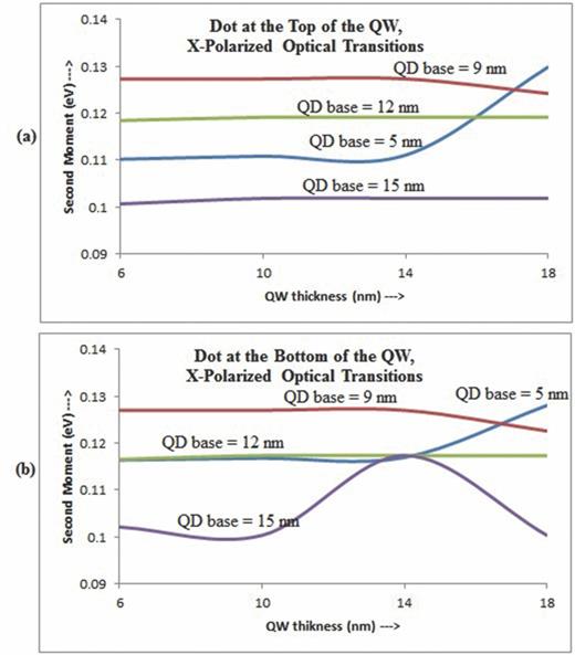
The second moments of the absorption spectra are shown for x-polarized light for two positions of the quantum dot: (a) at the top of the quantum well and (b) at the bottom of the quantum well. The sizes of the quantum dot are shown in the figure.
The second moments of the absorption spectra are shown for x-polarized light for two positions of the quantum dot: (a) at the top of the quantum well and (b) at the bottom of the quantum well. The sizes of the quantum dot are shown in the figure.

The second moments of the absorption spectra are shown for z-polarized light for two positions of the quantum dot: (a) at the top of the quantum well and (b) at the bottom of the quantum well. The sizes of the quantum dot are shown in the figure.
The second moments of the absorption spectra are shown for z-polarized light for two positions of the quantum dot: (a) at the top of the quantum well and (b) at the bottom of the quantum well. The sizes of the quantum dot are shown in the figure.
The ratio of the intensities of absorption peaks for x-polarized and z-polarized light as a function of the dot size and quantum well thickness is shown in Fig. 7. The results clearly show that for the dot size greater than 5 nm the intensity of the absorption line for x-polarized light is two orders of magnitude larger than the corresponding intensity for z-polarized light. Thus the DWELL structures are more sensitive to the x-polarized light.

Ratio of the intensities (Ix / Iz) for the DWELL system with the dot at the bottom of quantum well is shown as a function of the quantum dot size for different quantum well thicknesses.
Ratio of the intensities (Ix / Iz) for the DWELL system with the dot at the bottom of quantum well is shown as a function of the quantum dot size for different quantum well thicknesses.
Three color InAs/InGaAs quantum dots-in-a-well detector with wavelengths at 3.8 μm, 8.5 μm and 23.2 μm were reported in Ref. 28. In this paper, the shorter wavelengths (3.8 μm and 8.5 μm) are due to bound-to-continuum and bound-to-bound transitions between the states of the dot and states of the well. Our results show similar behavior with the absorption spectra in the wavelength range of 3.6 μm to 2 μm with the longer wavelength optical transition corresponding to the transitions between the states of the quantum dot.
The photodetector based on n-doped InAs/In0.15Ga0.85As dot-in-well structure has been studied experimentally in Ref. 29. The photodetector was operating at 78 K with the spectral response at 7.2 μm (170 meV) and with the spectral width of 35%. The peak was attributed to the bound to bound transitions between the ground state of the dot and the states of the well. In our single layer structure of doped InAs/In0.15Ga0.85As quantum dot-in-well photodetector with 1 electron/dot the response occurs in the range of 340 meV – 630 meV (1.9 μm – 3.6 μm) with an average spectral width of 20%. The corresponding intraband transitions are between the states of the quantum dot and the states of continuum (1.9 μm) and between the states of the dots (3.6 μm).
Two peaks at 4.2 μm and 7.6 μm have been reported by Krishna et al.30 for InAs/In0.15Ga0.85As quantum dot-in-well systrem with the average quantum dot height of 10 nm and base of 24 nm. From the photoluminescence measurements the group concluded that the intersubband transitions at 7.6 μm are due to bound to bound transitions between the states of the dot and the states of the well and the 4.2 μm are due to transitions between the states of the dot and continuum. It was also observed in Ref. 30 that the wavelength of the detector can be varied by changing the width of the quantum well, i.e. there is a significant increase in the cut-off wavelength of the detector (8 μm → 9 μm) as the thickness of the quantum well is increased by 2 nm. Our modeling shows that there is a weak dependence of the absorption spectra on the quantum well thickness. For example, for the quantum dot size of 9 nm the position of the absorption peak changes as 2.6 μm → 2.7 μm when the quantum well size increases from 14 nm to 18 nm.
Intersubband transitions in InAs/In0.15Ga0.85As quantum dot-in-well system were also reported in Ref. 31, where the peak operating wavelength was tailored from 7.2 μm to 11 μm at 60 K. Spectral response peaks were observed by this group at 10.3 μm and 11.3 μm under positive and negative bias, respectively. Both these peaks were attributed to bound-to-bound transitions between the InAs quantum dot and InGaAs quantum well. In these experiments the thickness of the quantum well was between 7 nm and 12 nm and the dot was on the top of the well. The peaks with the wavelength longer than 5.5 μm were identified with transitions between the ground state of the dot and the bound state in the well, which is consistent with our numerical results. Novel InAs/InGaAs quantum dots-in-well was reviewed by Sanjay Krishna32 in which the author was under the opinion that DWELL infrared photo detectors display normal incidence operation, bias-tunability and multicolor operation in the mid-wave infrared (3-5 μm), long-wave infrared (LWIR, 8-12 μm) and very long infrared (>14 μm) regimes. Also it was noted by the author that these detectors have low quantum efficiency, which translates into low responsivity and detectivity. The author suggested some methods to mitigate this problem such as replacing InAs/InGaAs/GaAs by InAs/GaAs/AlGaAs for having less strain in the multi-stack system.
The authors of Ref. 33 studied the interband and intersubband transitions of lateral InAs/In0.15Ga0.85As/GaAs dots-in-well infrared photodetectors and concluded that the origin of the photocurrent was due to intersubband transitions between the quantum dot ground state and the quantum well excited state, which is consistent with our results discussed above. The authors of Ref. 33 used InAs quantum dots caped with 3 nm In0.15Ga0.85As quantum wells and a 30 nm GaAs barrier for their studies of the origin of photo current.
A theoretical study of DWELL system was performed by Nenad Vukmorivic et al.34 in order to understand the origin of change of the operating wavelength of DWELL photodetectors when the well thickness is varied. Similar to our finding, the authors of Ref. 34 concluded that the changes of the quantum well thickness cannot be responsible for the shifts of the absorption peaks observed in the experiments of Ref. 31. Other properties of DWELL photodetectors, such as generation of the photocurrent, the bias dependence of the photoresponse, and variation of the composition of DWELL system, were also studied both theoretically and experimentally.35–39 In the present paper the conduction band mass of In0.15Ga0.85As, InAs and GaAs were taken from Ref. 40.
IV. CONCLUSION
We study the intraband optical spectra of n-doped InAs/InxGa1-xAs/GaAs DWELL system for different sizes of quantum dot and quantum well. The spectra are obtained for two different positions of the dot in the well: dot at the bottom and at the top of the well. Our results show that absorption spectra have weak dependence on the quantum well size and on the position of the dot in the well. The spectra have strong dependence on the dot size. For smaller sizes of the quantum dot, b < 12 nm, the main optical transitions occur either between the states of the quantum dot and the quantum well or between the states of the quantum dot and substrate. The wavelengths of corresponding optical transitions range between ∼2 μm and ∼3.6 μm. Such types of optical transitions are specific for DWELL system and are not present in isolated quantum dot.
The DWELL system is sensitive to both x- and z-polarized light. For x-polarized light the absorption spectra have multi-peak structure with well-defined peaks of comparable intensities. For z-polarized light, the absorption spectrum has only one peak. The DWELL system is more sensitive to x-polarized light, for which the intensity of the optical transitions is almost two orders of magnitude larger than the corresponding intensities for z-polarized light.

