


Introduction
Electronic devices and systems have become increasingly more complex throughout their evolutionary history owing to demands for high-performance and multi-functionality. Therefore, electromagnetic interference (EMI) and compatibility have emerged as key issues when equipment design for commercial or military purposes is concerned [Reference Yaghjian1, Reference Tong, Thomas, Biwojno, Nothofer, Sewell and Christopoulos2]. Providing reliable information regarding the electric and magnetic field in the near-field of integrated circuit chips and printed circuit boards is of a particular importance in resolving these issues. An intentional emission from antennas and unintentional emission from electronic equipment are usually characterized by an established technique known as the near-field scanning measurement [Reference Ravelo, Liu and Jastrzebski3–Reference Tian, Li, Liu, Wan and Cao5].
Near-field probes make the essential parts of near-field measurement procedure generally used to characterize either deterministic or stochastic electromagnetic (EM) fields.
In general, the output from the probe can be simply considered as directly proportional to the field intensity at the probe position, without taking into account the influence of the probe on the field being measured. Nevertheless, measured values may experience some deviations as a result of the probe itself and, additionally, the probe output might be affected by its directional characteristics. Therefore, an appropriate calibration procedure of the near-field scanning probes becomes a necessity, with the purpose of realistic parameters extraction through compensation of the probe influence. If it is determined correctly, the calibration characteristic is further used to correct the measured output, that is to say, the probe influence would be removed and the final result would correspond to the realistic field that would have existed in the absence of the probe. Successfully calibrated near-field probes are particularly important in recently proposed approaches for an efficient characterization of stochastic EM fields [Reference Russer and Russer6–Reference Haider, Stošić, Baharuddin, Dončov, Thomas, Russer and Russer8], where two-point measurements for capturing the correlation information should be applied. This procedure may require probes of different diameters depending on which height from a device under test (DUT) the scanning is performed or it may be imposed that the probes are very close to each other due to the required resolution of a scanning plane.
Kerns proposed one of the approaches for the probe corrections in [Reference Kerns9]. Some miniaturized magnetic-field probes have been reported for measurements in high-frequency planar circuits [Reference Gao, Lauer, Ren and Wolff10]. Formulations of probe-corrected planar near-field scanning in both frequency and time domains have been proposed by Hansen and Yaghjian [Reference Hansen and Yaghjian11]. A probe calibration is performed by means of a TEM-cell measurement and the use of near-field probes is also characterized in a theoretical way by [Reference Criel, Haelvoet, Martens, De Zutter, Franchois, De Smedt and De Langhe12]. The influence of the measurement probe on the evaluation of the far- and near-field of an EM source is characterized in [Reference Joseph and Martens13]. Shi applied the theory of probe-compensated near-field measurement by applying the Lorentz reciprocity theorem to the problem of characterizing EMI through the use of near-field scanning measurements [Reference Gao and Wolff14, Reference Shi, Cracraft, Slattery, Yamaguchi and DuBroff15].
The work presented herein describes the generation of the calibration characteristic of the loop probe used in the near-field scanning measurements [Reference Dimitrijevic, Atanaskovic, Doncov, Thomas, Smartt and Baharuddin16], characterization of the tangential magnetic field in the scanning area, and additional correction of the calibration curve in case of stochastic field measurement with two scanning probes. The novelty of this paper relates to the two-point measurement procedure performed with two loop probes which are generally used for characterization of stochastic EM fields. Bearing in mind that the coupling between probes is in these scenarios inescapable, here it is actually demonstrated how an additional scanning probe affects the measured field values. This coupling could be especially important in cases when different probe orientations are needed to capture both tangential field components during the near-field scanning, mostly affecting the accurate calculation of neighboring cross-correlation elements of the field–field correlation matrix.
As a testing board, a simple 50 Ω microstrip line is used and the calibration characteristic of the loop probe is obtained according to the near-field measurement and full-wave simulation results at specific points above the DUT. Near-field measurements are conducted in the close scanning area at the specific height above the line, specifically along the line itself and across the line, and the measured output is transformed into the magnetic field using the probe calibration factor. The calculated magnetic field is then compared with the fields predicted by full-wave simulations. Based on the measurements and simulations carried out with two loop probes, corrections representing the influence of additional loop probe on the single probe output level are illustrated. All of the simulations, measurements, and calibration are performed in the frequency domain.
Near-field scanning measurement set-up
The near-field measurement system is comprised of a 3-D positioning system, scanning probe, a test structure, vector network analyzer (VNA – Vector Network Analyzer E5062A, up to 3 GHz), and cables. The block diagram and the experimental setup for the measurements in the frequency domain along with the 3-D positioning system are shown in Fig. 1. The measurement setup allows measuring S-parameters of the probe over the test structure.

Fig. 1. (a) Block diagram of the frequency-domain measurement setup. (b) Experimental set-up (PC with LabVIEW and VNA). (c) 3-D positioning system.
The terminated microstrip test board was realized to be used as a test structure, since the field distribution above this microstrip calibration board can be determined easily by approximate analytical solutions or a full-wave simulation. A 50 Ω microstrip line was fabricated on FR4 substrate with characteristics: substrate relative permittivity εr = 4.35, substrate height h = 1.6 mm, the line width w = 3.05 mm, and the line length l = 160 mm (Fig. 2(a)). As a near-field probe, a passive H-field loop probe LANGER RF-R 50-1 with the head size diameter of 10 mm (https://www.langer-emv.de) was used (Fig. 2(b)). The frequency-domain measurement was conducted automatically using a relevant MATLAB code in conjunction with the LabVIEW environment in the anechoic chamber of the George Green Institute of Electromagnetic Research (GGIEMR) at the University of Nottingham.

Fig. 2. (a) Test microstrip line. (b) Test board and the RF-R 50-1 loop probe placed above the board in the anechoic chamber.
Calibration procedure
A probe calibration procedure is carried out in order to characterize the presence of a near-field scanning probe and its impact on measured near-field values. Measuring the voltage signal from a loop probe, Up, and obtaining the magnetic field via a full-wave simulation, Hsim, enable the probe calibration factor to be determined as

In the measurement setup for the calibration procedure, the scanning probe is fixed at the height z = 10 mm above the center of the microstrip line (x = 0, y = 0). The line is placed along the x-axis, x = (−80 to 80) mm, with one terminal connected to the output port of the VNA, while the other terminal is terminated with 50 Ω. The input port of the VNA is connected to the loop probe. The input power of the test line is set to 0 dBm, and the measurements are performed in the frequency range 10 MHz to 3 GHz. Data obtained by VNA correspond to the S 21 parameter of two ports, which can be further manipulated to obtain the probe's response as the voltage, which is needed for calculation of the probe calibration factor.
In addition, a model of the microstrip line is constructed in the full-wave simulator and simulated results representing the y component of the magnetic field in the point that would correspond to the center of the loop probe in the same frequency domain are obtained.
Figure 3 presents the probe calibration factor versus frequency calculated using the voltage on the loop probe and the simulated magnetic field at the position of the probe in the measurement setup. The voltage is determined from the measured S 21 on the VNA, while the field is obtained via the TLM method in the CST Studio Suite. Both voltage and simulated magnetic field are plotted in the figure. It can be seen that a good agreement is achieved between the calculated CF and the data given by the manufacturer (https://www.langer-emv.de).

Fig. 3. The probe calibration factor, the simulated y component of the magnetic field, and the measured voltage.
Experimental and numerical results
In order to explore the accuracy of the probe calibration factor, a set of measurements were performed using the same measurement setup and the same microstrip line. The loop, placed at the fixed height 10 mm above the center of the line, was moved along and across the line to take data at 121 and 61 points, respectively, mutually separated by 1 mm. The measured S 21 output of each point was transformed to give received voltage which was then corrected by the probe calibration factor, and as a result, the y component of the magnetic field produced by the microstrip trace is calculated. Corresponding full-wave simulations were conducted accordingly. Figure 4 illustrates 2-D plots of the measured Hy field component as the function of a position and a frequency for the scanning loop positions in the xy plane at the height z = 10 mm above the line which are distributed across and along the line.
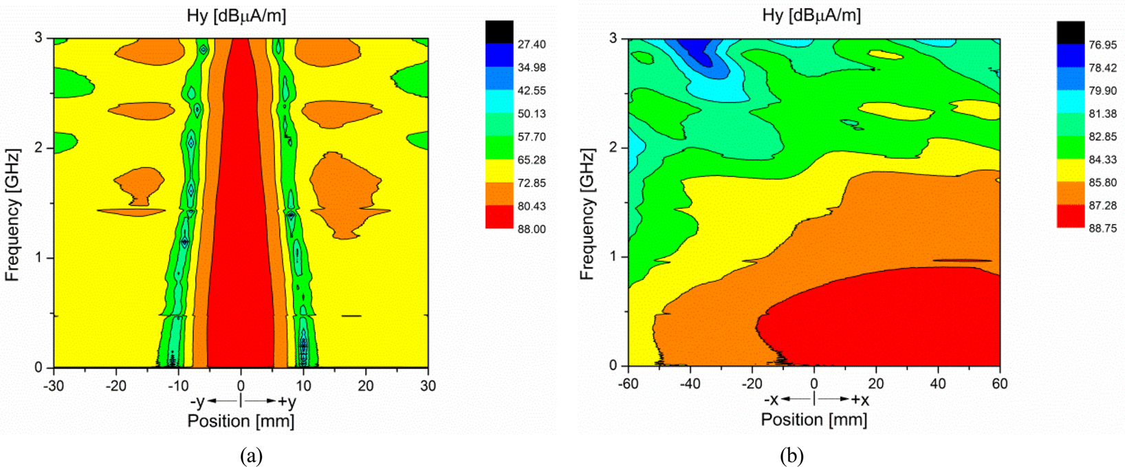
Fig. 4. Measured Hy field component as a function of the position and the frequency for the loop positions: (a) x = 0, y = (−30 to 30) mm, z = 10 mm; (b) x = (−60 to 60) mm, y = 0, z = 10 mm.
Figures 5 and 6 present the comparison between simulated and measured results of the Hy field with the probe calibration included, in positions across the line and along the line, respectively, for six frequency values in the considered frequency range. As can be observed, a satisfactory agreement is achieved. The highest Hy field component values are observable along the line in x-direction, whereby the relevant area is dependent on the frequency. In practice, it is difficult to achieve the ideal matching of the microstrip line, so that there is a slight variation of the magnetic field along the line, which can be seen in Figs 4(b) and 6.

Fig. 5. Simulated and measured Hy field component at positions x = 0, and y = (−30 to 30) mm, z = 10 mm.

Fig. 6. Simulated and measured Hy field component at positions x = (−60 to 60) mm, and y = 0 mm, z = 10 mm.
Influence of an additional loop probe on measurement results
This section is devoted to the near-field measurements of a test microstrip line using a loop probe, placed at the fixed position, in the presence of an additional loop probe which position was varied in a scanning area. The purpose of this investigation was to consider the influence of a second probe on near-field measurement results since the near-field measurements in stochastic scenarios are generally carried out by using two or more loop probes, where the coupling between them is inevitable.
Measurements in the frequency domain were performed in the anechoic chamber using the VNA, while two RF loop probes R 50-1 were used as scanning probes. The automated measurement was operated using the MATLAB code in conjunction with LabVIEW environment. The fixed loop probe was placed at the height 10 mm above the center of the line and terminated with the 50 Ω load (Fig. 7(a)). The scanning plane was just one-quarter of the (160 × 80) mm board size due to symmetry, and it was divided into 31 × 21 points mutually separated by 2 mm (Fig. 7(b)). Measured values of transmission coefficient between a loop probe and a microstrip line input in the presence of an additional loop probe in different positions are depicted in Fig. 8. The starting position of the second, x = 0 mm, y = 0 mm, corresponds to the label x-01, y-01 in Fig. 8(b). In regards to that point, the fixed probe is placed at a distance of 2 mm along the y-axis while the position along the x-axis is the same. It can be found that the transmission coefficient has the lowest values for the positions of the additional probe which are closest to the primary loop probe, hence the effect of the additional probe in these positions is the most conspicuous.

Fig. 7. (a) Near-field measurements with the scanning probe in the presence of the second loop probe. (b) Scanning area layout with defined positions of the second probe which position is changed.

Fig. 8. Measured transmission coefficient between a loop probe and a microstrip line input in the presence of the additional loop probe for different second probe's positions.
Corresponding simulations were carried out in CST Studio Suite, and for this purpose, both loop probes were designed and included in the model at the appropriate positions in order to obtain Hy field in a realistic situation. The influence of the second probe on output results is illustrated through the correction factor of the transmission coefficient between a loop probe and an input into the microstrip line, obtained by measurements and simulations, in Fig. 9. The correction factor is determined through comparing the calibration factor reached in the presence of the additional probe and the calibration factor obtained with only one scanning probe. Apparently, as the distance between two probes is increased, the second probe's effect is reduced. The correction factor has the value around 1.5 dB when the second probe is placed at the distance up to 5 mm from the fixed probe along y-axis and up to 10 mm along the x-axis. For greater separation between probes, the correction factor becomes almost negligible with the value smaller than 0.2 dB.

Fig. 9. Correction factor of measured and simulated transmission coefficient at different frequencies. (a) Measured at 500 MHz, (b) simulated at 500 MHz, (c) measured at 1000 MHz, (d) simulated at 1000 MHz, (e) measured at 1500 MHz, (f) simulated at 1500 MHz, (g) measured at 2000 MHz, (h) simulated at 2000 MHz, (i) measured at 2500 MHz, (j) simulated at 2500 MHz, (k) measured at 3000 MHz, (l) simulated at 3000 MHz.
Given results correspond to the case when the first scanning probe is fixed in one position. For two-point stochastic field measurements, the position of the first probe is also changed, but it is fixed when the position of the second probe varies. Bearing in mind that the biggest coupling between two probes is found when they are close to each other and under the estimation that the field can be considered uniform in the small area around the probe, it is worth to conclude that the given estimation of the correction factor would be also relevant with significant accuracy for other positions of the first scanning probe.
Conclusion
This paper presents a procedure for calibration of near-field scanning probes based on the measurement setup with a microstrip line as a test structure and a loop probe as a scanning probe. The same setup is intended to be further used for characterization of the field correlation of devices with uncorrelated sources that have a stochastic field distribution. The calibration procedure described here can be used to eliminate the measurement error and it represents the first step in an investigation related to the measurement of stochastic EM fields using two scanning probes. The given calibration procedure has been amended with the research of an additional scanning probe influence on the measured results which will allow for the efficient and accurate near-field measurement of the radiated emissions from electronic equipment.
Future investigations will be focused on the design of the relevant models of a near-field probe starting from its simple form as a wire structure to more complex semi-rigid coax cable shape which will be compared with the lumped element model. In such a way, the numerical model will fully resemble the near-field measurement procedure and it can contribute to the improvement of the near-field image resolution in space, time, and frequency domains.
Acknowledgements
This work was supported by the Ministry of Education, Science and Technological Development of Serbia, project numbers TR32052, III 44009, and COST Action IC1407, and in part by the Geran Universiti Penyelidikan UKM (GUP-2019-021). The work was also supported through the provision of a cooperation license for the CST Studio Suite within 3DS Simulia by Dassault Systemes.
 Tijana Dimitrijević was born in Nis, Serbia, in 1977. She received the Dipl.-Ing., M.Sc., and Ph.D. degrees from the Faculty of Electronic Engineering, University of Nis, Serbia, in 2003, 2007, and 2015, respectively. From 2003 to 2008, she was a Researcher, from 2008 to 2010 Junior Teaching Assistant, and from 2010 she is a Teaching/Research Assistant at the Department of Telecommunications, University of Nis, Serbia. She joined the George Green Institute for Electromagnetics Research, the University of Nottingham, UK as a Research Fellow in December 2019. Her main research interests include computational electromagnetics, in particular the development and application of time-domain numerical methods (TLM and UTLM) for RF/microwave applications, with an emphasis on antenna design. She was the recipient of the Nikola Tesla National Award in Creativity of the Young category by the Republic of Serbia Ministry of Science in 2006, and the recipient of the Aleksandar Marinčić Award by Serbian MTT Society for the extraordinary scientific achievements in 2017.
 Aleksandar Atanaskovic received the Dipl. Ing., M.Sc., and Ph.D. degrees in electrical engineering from the Faculty of Electronic Engineering, University of Niš, in 1997, 2004, and 2015, respectively. In November 1997, he joined the Faculty of Electronic Engineering, University of Niš, where he is currently a Teaching Assistant at the Department of Telecommunications. His research interests include the fields of automatization of measurement systems, microwave active and passive circuits, microwave and RF power amplifiers, and linearization techniques.
 Nebojša S. Dončov received the Dipl.-Ing., M.Sc., and Ph.D. degrees from the Faculty of Electronic Engineering, University of Nis, Serbia, in 1995, 1999, and 2002, respectively. From 1998 to 2001, he was a Research Assistant with the Faculty of Electronic Engineering, University of Niš. From 2001 to 2004, he was a Research and Development Engineer with the Electromagnetics Division of Flomerics Ltd., Nottingham, UK. Since 2004, he has been with the Department of Telecommunications, Faculty of Electronic Engineering, University of Niš where he is now a Full Professor. His research interests include computational and applied electromagnetics with a particular emphasis on TLM and network methods applications in microwaves, antennas, and EMC. Dr. Dončov was a recipient of the International Union of Radio Science (URSI) Young Scientist Award in 2002.
 David W. P. Thomas is a Professor of Electromagnetics Applications in The George Green Institute for Electromagnetics Research, The University of Nottingham UK. His research interests are in electromagnetic compatibility, electromagnetic simulation, power system transients, and power system protection. He is a member of CIGRE and convenor for Joint Working Group C4.31 “EMC between communication circuits and power systems”, Chair of COST Action IC 1407 “Advanced Characterisation and Classification of Radiated Emissions in Densely Integrated Technologies (ACCREDIT)”, a member of several conference committees the EMC Europe International Steering Committee. He is a Vice chair of IEEE Standards committee P2718 Guide for Near Field Characterization of Unintentional Stochastic Radiators.
 Christopher Smartt received the M.Eng. and Ph.D. degrees in Electrical and Electronic Engineering from the University of Nottingham in 1991 and 1995, respectively. Following 2 years working as a Research Assistant at the University of Nottingham, he joined BAE SYSTEMS where he worked on 2-D and 3-D full-field time-domain techniques for electromagnetic field simulation for aerospace applications. In 2007, he re-joined the George Green Institute For Electromagnetics Research at the University of Nottingham as a Research Fellow where his research interests include the development and application of computational electromagnetics methods and the development of techniques for time-domain measurement of electromagnetic fields including near-field methods, with applications to EMC and EMI studies.
 Mohd Hafiz Baharuddin was born in Kelantan, Malaysia, in January 1987. He received the B.Eng. degree in Electrical and Electronic Engineering and the M.Eng. degree in Electrical Engineering from Stevens Institute of Technology, Hoboken, NJ, USA, in 2009 and 2011, respectively. He completed his Ph.D. degree in Electrical and Electronic Engineering with the University of Nottingham, Nottingham, UK in 2019. He is currently working as a lecturer at the Universiti Kebangsaan Malaysia, Malaysia. His research interests include modeling and experimental methods in electromagnetic compatibility focusing on the characterization of the stochastic electromagnetic fields in the near field.


 Open access